Compound for organic electronic element, organic electronic element using the same, and an electronic device thereof

a technology of electronic elements and organic electric elements, which is applied in the direction of luminescent compositions, isotope introduction to heterocyclic compounds, organic chemistry, etc., can solve the problems of power consumption, efficiency and life span, and the need to increase the need for power consumption, so as to improve luminescence efficiency, color purity and lifespan, the effect of improving the efficiency of luminescen

Active Publication Date: 2017-05-04
DUK SAN NEOLUX
View PDF3 Cites 40 Cited by
  • Summary
  • Abstract
  • Description
  • Claims
  • Application Information

AI Technical Summary

Benefits of technology

[0017]In order to solve one or more of the above-mentioned problems occurring in the prior art, an aspect of the present invention is to provide a compound which allows an organic electric element to improve in luminescence efficiency, stability and lifespan, an organic electric element containing the same, and an electronic device including the organic electric element.
[0020]By employing the compound of the present invention, the organic electric element according to one or more embodiments of the present invention can have improved luminescence efficiency, high heat-resistant, color purity and lifespan.

Problems solved by technology

Currently, the power consumption is required more and more as size of display becomes larger and larger in the portable display market.
Therefore, the power consumption is a very important factor in the portable display with a limited power source of the battery, and efficiency and life span issue also must be solved.
However, efficiency cannot be maximized only by simply improving the organic material layer.
However, it mainly has a low T1 value because a material used in a hole transporting layer should have a low HOMO value, thereby excitons generated from a light emitting layer are transported to the hole transporting layer, resulting in a charge unbalance in the light emitting layer.
Thus, light emission occurs in the hole transporting layer or at an interface of the hole transporting layer so that color purity, efficiency and lifespan of the organic electroluminescent device are reduced.
Further, when a material with rapid hole mobility is used in order to reduce a driving voltage in the organic electroluminescent device, it shows tendency to lower the efficiency.
This causes a charge unbalance in the light emitting layer resulting in low emitting efficiency and lifespan.
However, such a stable and efficient organic material layer material for an organic electric element has not yet been fully developed.

Method used


Image

  • Compound for organic electronic element, organic electronic element using the same, and an electronic device thereof
  • Compound for organic electronic element, organic electronic element using the same, and an electronic device thereof
  • Compound for organic electronic element, organic electronic element using the same, and an electronic device thereof

Examples


synthesis example

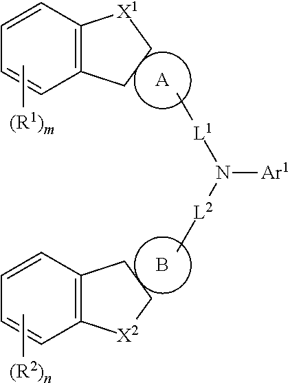
[0085]The compounds (final products) of the present invention represented by Formula 1 can be synthesized by reaction of Sub 1 and Sub 2 as illustrated in, but not limited to, the following Reaction Scheme 1.

[0086](X1, X2, A ring, B ring, Ar1, L1, L2, R1, R2, m and n are each the same as defined in Formula 1 above.)

[0087]I. Synthesis of Sub 1

[0088]Compound Sub 1 of Reaction Scheme 1 can be synthesized, but not limited to, by any one reaction of the following Reaction Schemes 2 to 4.

[0089]In Reaction Schemes 2 to 4, R corresponds to (R1)m or (R2)n of Formula 1, X corresponds to X1 or X2 of Formula 1, L corresponds to L1 or L2 of Formula 1, and Z ring corresponds to A ring or B ring of Formula 1.

[0090]Synthesis Examples of compounds comprised in Sub 1 are as followings.

1. Synthesis Example of Sub 1-10

[0091]

[0092]2-(4-bromophenyl)-1-(methylsulfinyl)naphthalene (35.08 g, 101.6 mmol) as a starting material and triflic acid (134.9 ml, 1524.1 mmol) were loaded into a round bottom flask and...

example 1-2

[Example 1-2] to [Example 1-65] Green OLED (a Hole Transport Layer)

[0214]The OLEDs were manufactured in the same manner as described in Example I-1, except that any one of the compounds P-4 to P-200 of the present invention in the Table 4 below was used as the hole transport layer material of the light emitting layer, instead of the inventive compound P-1.
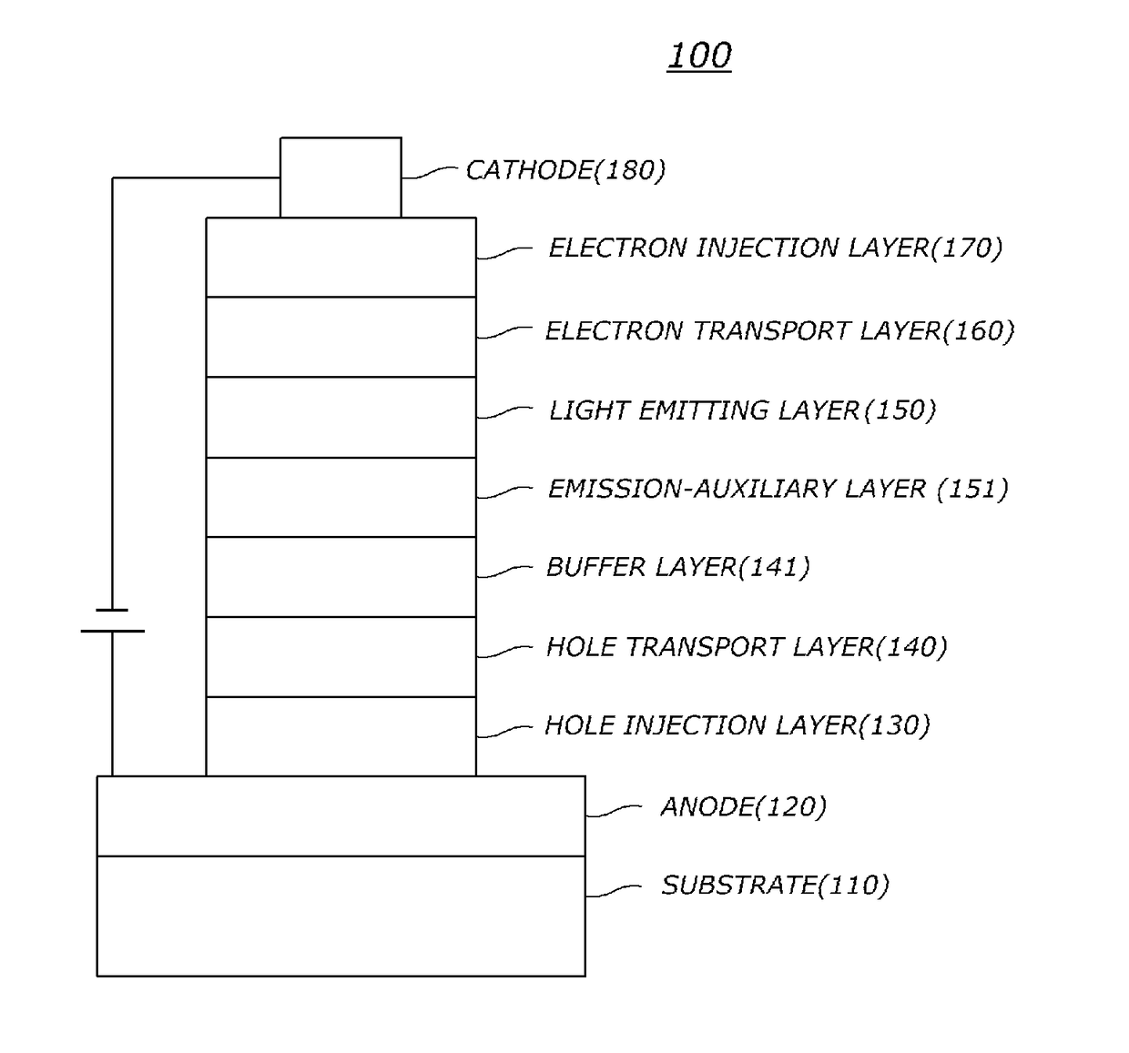
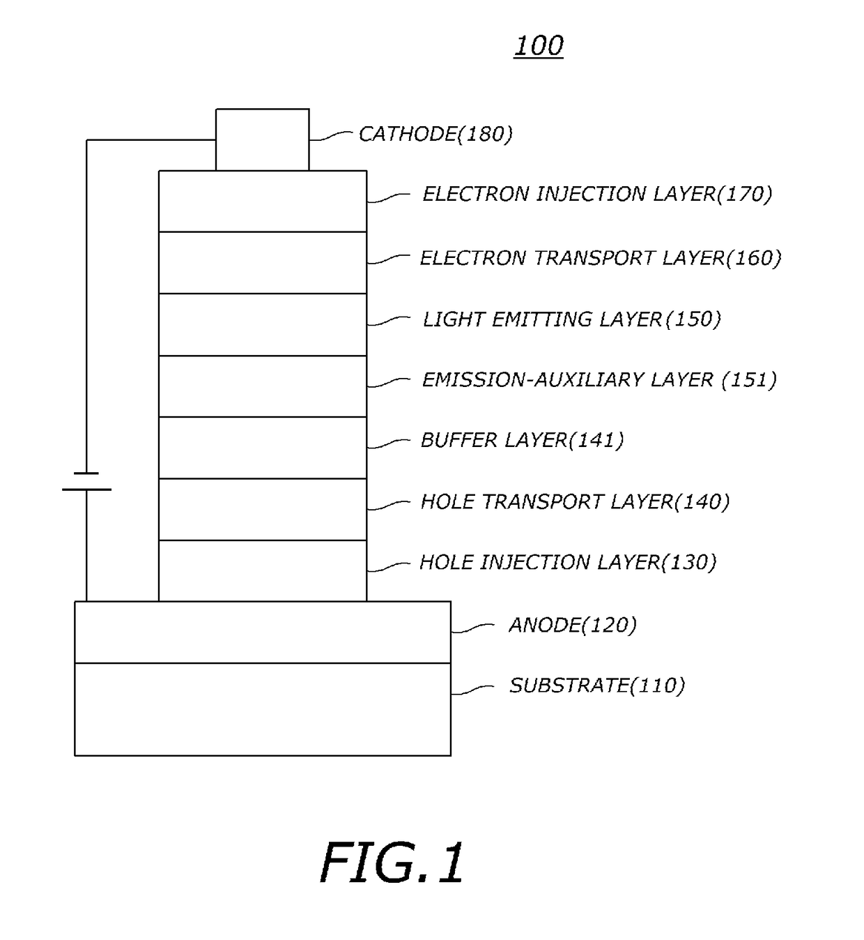
example ii-1

[Example II-1] Green OLED (an Emission-Auxiliary Layer)

[0225]Organic light emitting diodes (OLEDs) were fabricated according to a conventional method by using a compound of the present invention as an emission-auxiliary layer material.

[0226]First, an ITO layer (anode) was formed on a glass substrate, and then 2-TNATA was vacuum-deposited on the ITO layer to form a hole injection layer with a thickness of 60 nm.

[0227]Subsequently, N,N′-Bis(1-naphthalenyl)-N,N′-bis-phenyl-(1,1′-biphenyl)-4,4′-diamine (hereinafter, “NPB”) was vacuum-deposited with a thickness of 60 nm on the hole injection layer to form a hole transport layer.

[0228]Subsequently, the compound P-1 of the present invention was vacuum-deposited on the hole transport layer to form an emission-auxiliary layer with a thickness of 20 nm. A light emitting layer with a thickness of 30 nm was formed on the emission-auxiliary layer by using the CBP as a host material and Ir(ppy)3 as a dopant material in a weight ratio of 90:10.

[02...


PUM

PropertyMeasurementUnit
thicknessaaaaaaaaaa
thicknessaaaaaaaaaa
thicknessaaaaaaaaaa

Abstract

Provided are a compound of Formula 1 and an organic electric element including a first electrode, a second electrode, and an organic material layer between the first electrode and the second electrode and comprising the compound, the element showing improved luminescent efficiency, stability, and life span.

Description

CROSS-REFERENCE TO RELATED APPLICATION[0001]This patent application claims benefit under 35 U.S.C. 119, 120, 121, or 365, and is a National Stage entry from International Application No. PCT / KR2015 / 005877, filed Jun. 11, 2015, which claims priority to Korean Patent Application No. 10-2014-0074261 filed on Jun. 18, 2014, the contents of which are hereby incorporated by reference for all purposes as if fully set forth herein.BACKGROUND[0002]Technical Field[0003]The present invention relates to compounds for organic electric elements, organic electric elements comprising the same, and electronic devices thereof.[0004]Background Art[0005]In general, an organic light emitting phenomenon refers to a phenomenon in which electric energy is converted into light energy of an organic material. An organic electric element utilizing the organic light emitting phenomenon usually has a structure including an anode, a cathode, and an organic material layer interposed therebetween. In many cases, th...

Claims


Application Information

Patent Timeline
Patent Type & Authority Applications(United States)
IPC IPC(8): H01L51/00C07B59/00C07D333/74C07D409/12
CPCH01L51/0061C07D409/12C07B59/002C07D333/74H01L51/006C07B2200/05H01L51/0074H01L51/0052H01L51/0054H01L51/0058H01L51/0073H01L51/5056C07D333/76C07D307/91C09K11/06C09K2211/1022C09K2211/1088C09K2211/1092Y02E10/549H10K85/636H10K85/633H10K85/631H10K85/615H10K85/324H10K85/6576H10K85/6574H10K85/342H10K50/156H10K50/15C07D333/50C07D307/77H10K50/11H10K50/17H10K85/622H10K85/626
Inventor LEE, BUM SUNGCHOI, YEON HEEPARK, JUNG CHEOLPARK, YONG WOOKJI, HEE SUNKANG, MOON SUNGYEO, SEUNGWON
Owner DUK SAN NEOLUX
Why Eureka
Try Eureka