
Performing planarization process controls in semiconductor fabrication

a semiconductor and process control technology, applied in semiconductor/solid-state device testing/measurement, lapping machines, instruments, etc., can solve the problems of increasing the complexity of processing and manufacturing ics, slurry has corrosive properties and chemically etches the wafer, and conventional cmp process control methods have not analyzed byproduct components generated during a cmp process, etc. problems

Active Publication Date: 2019-11-05
TAIWAN SEMICON MFG CO LTD
View PDF20 Cites 0 Cited by
  • Summary
  • Abstract
  • Description
  • Claims
  • Application Information

AI Technical Summary

Benefits of technology

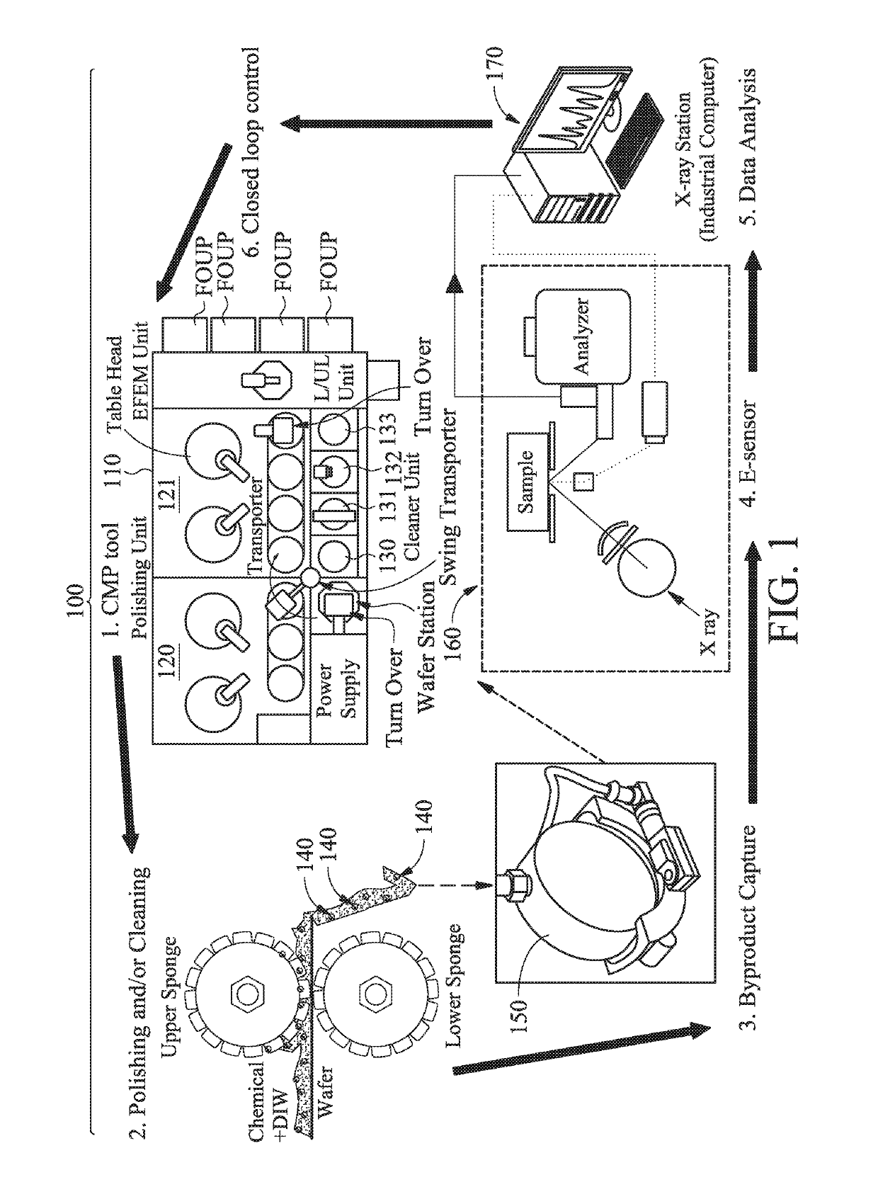
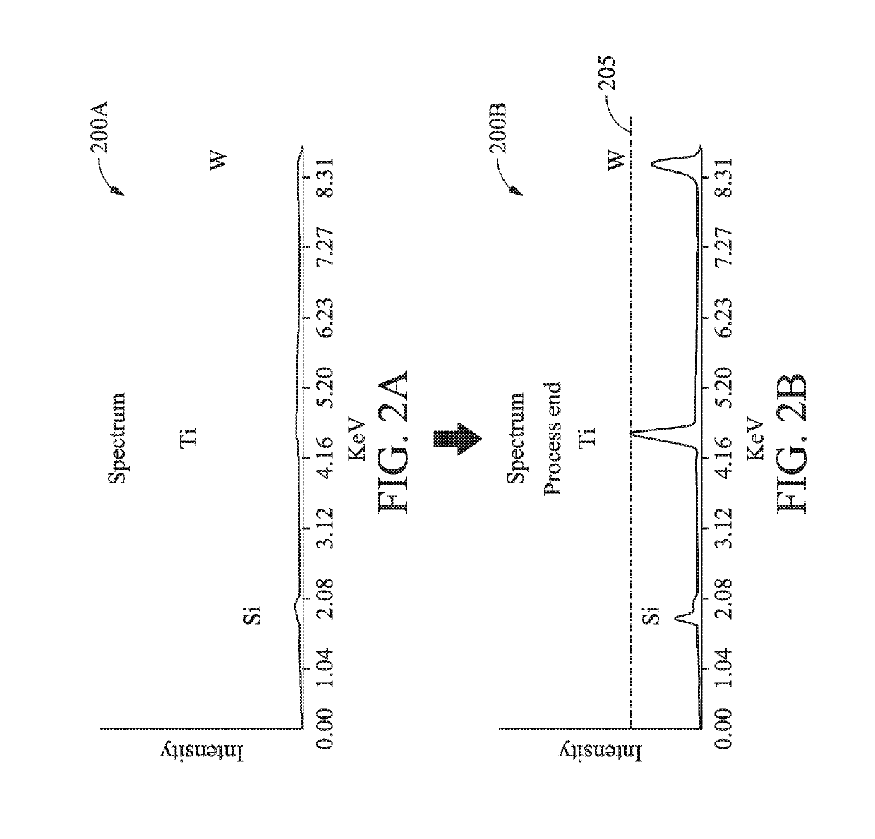
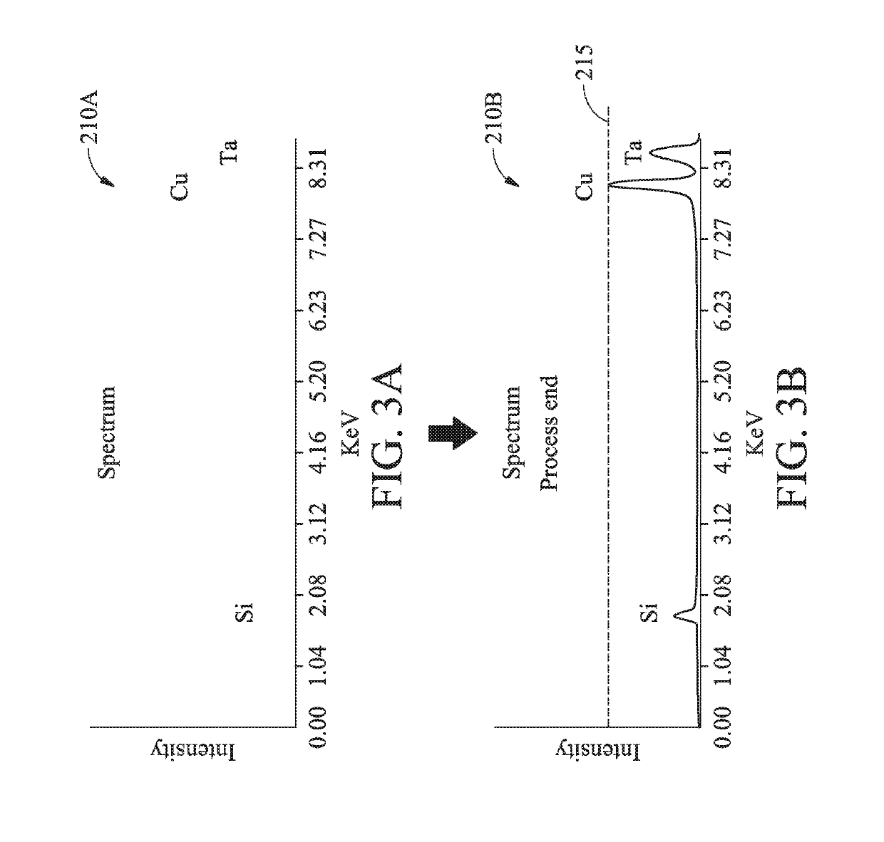
[0074]The present disclosure offers advantages over conventional methods of performing planarization processing control. It is understood, however, that other embodiments may offer additional advantages, and not all advantages are necessarily disclosed herein, and that no particular advantage is required for all embodiments. Conventional planarization methods such as CMP may rely on parameters such as polishing time or polishing rate for endpoint detection. However, these endpoint detection methods are not sufficiently accurate, and as a result the wafer may be over-polished or under-polished (or over-cleaned or under-cleaned). In comparison, the CMP processing controls of the present disclosure collect and analyze CMP byproduct samples and perform end-point detection based on the CMP byproduct analysis. This allows for more accurate end-point detections for both the polishing and cleaning processes associated with CMP. In addition, the CMP byproduct analysis may also reveal errors or problems with the CMP process, for example by detecting the presence of unknown elements in the CMP byproduct, or a stronger-than-expected presence of an element (even if that element itself is expected) in the CMP byproduct, or an unexpected chronological order in which expected elements appear in the CMP byproduct. As such, problems can be corrected promptly and will not significantly impact yield or device performance negatively. The processes and systems of the present disclosure are also compatible with existing process flow and thus are not costly to implement.

Problems solved by technology

However, these advances have increased the complexity of processing and manufacturing ICs and, for these advances to be realized, similar developments in IC processing and manufacturing are needed.
The slurry has corrosive properties and chemically etches the wafer.
However, conventional CMP process control methods have not analyzed byproduct components generated during a CMP process, or use the byproduct component analysis for purposes of CMP process control.
Therefore, although existing methods and systems of performing planarization processes such as CMP have been generally adequate for their intended purposes, they have not been entirely satisfactory in every aspect.

Method used


Image

  • Performing planarization process controls in semiconductor fabrication
  • Performing planarization process controls in semiconductor fabrication
  • Performing planarization process controls in semiconductor fabrication

Examples


Embodiment Construction

[0011]It is understood that the following disclosure provides many different embodiments, or examples, for implementing different features of the invention. Specific examples of components and arrangements are described below to simplify the present disclosure. These are, of course, merely examples and are not intended to be limiting. For example, the formation of a first feature over or on a second feature in the description that follows may include embodiments in which the first and second features are formed in direct contact, and may also include embodiments in which additional features may be formed between the first and second features, such that the first and second features may not be in direct contact. In addition, the present disclosure may repeat reference numerals and / or letters in the various examples. This repetition is for the sake of simplicity and clarity and does not in itself dictate a relationship between the various embodiments and / or configurations discussed. M...


PUM

PropertyMeasurementUnit
timeaaaaaaaaaa
time deltasaaaaaaaaaa
energyaaaaaaaaaa

Abstract

A planarization process is performed to a wafer. In various embodiments, the planarization process may include a chemical mechanical polishing (CMP) process. A byproduct generated by the planarization process is collected and analyzed. Based on the analysis, one or more process controls are performed for the planarization process. In some embodiments, the process controls include but are not limited to process endpoint detection or halting the planarization process based on detecting an error associated with the planarization process.

Description

PRIORITY DATA[0001]This application claims priority from U.S. Provisional Patent Application No. 62 / 592,587, entitled “Performing Planarization Process Controls based on Captured Byproduct Samples” and filed on Nov. 30, 2017, the disclosure of which is incorporated herein in its entirety.BACKGROUND[0002]The semiconductor integrated circuit (IC) industry has experienced rapid growth. Technological advances in IC materials and design have produced generations of ICs where each generation has smaller and more complex circuits than the previous generation. However, these advances have increased the complexity of processing and manufacturing ICs and, for these advances to be realized, similar developments in IC processing and manufacturing are needed. In the course of integrated circuit evolution, functional density (i.e., the number of interconnected devices per chip area) has generally increased while geometry size (i.e., the smallest component (or line) that can be created using a fab...

Claims


Application Information

Patent Timeline
Patent Type & Authority Patents(United States)
IPC IPC(8): H01L21/321G01N23/20G06F11/07H01L21/66B24B37/013G01N1/10
CPCG01N23/20075G06F11/07H01L22/26H01L21/3212G01N1/10B24B37/013H01L21/02043H01L21/304H01L21/67028H01L21/67092H01L21/67276
Inventor CHEN, CHUNHUNGWANG, SHENG-CHENCHUANG, CHIN WEI
Owner TAIWAN SEMICON MFG CO LTD
Learn More