X-ray thin film inspection device

a thin film inspection and x-ray technology, applied in the direction of radiation beam directing means, instruments, radiation diffraction-based material analysis, etc., can solve the problems of insufficient precision for thin film measurements of several nm, inability to install cross-sectional transmission electron microscopes in in-line manufacturing processes and inspect thin films, etc., to achieve the effect of reducing background (bg) components

Active Publication Date: 2019-11-12
RIGAKU CORP
View PDF9 Cites 14 Cited by
  • Summary
  • Abstract
  • Description
  • Claims
  • Application Information

AI Technical Summary

Benefits of technology

[0005]Therefore, the applicant of the present application has proposed an X-ray thin film inspection device that can be installed in a process of manufacturing film-formed products, directly inspect the products themselves and can inspect even a thin film of several nm with sufficient precision without discarding a wafer after use (see Patent Document 1: JP-A-2006-153767).
[0020]The slit mechanism is preferably provided with two shielding plates formed of a material for shielding X-rays, and configured to pass the arbitrary number of focused X-ray beams through a gap formed between the shielding plates, and has a function of freely adjusting the extent of the gap.
[0037]Accordingly, scattered X-rays from air, ghost from a reflection mirror, etc. can be shielded by the X-ray shielding member or the receiving slit, and incidence of these X-rays other than the reflected X-rays to the one-dimensional X-ray detector can be suppressed, whereby the background (BG) components can be reduced.

Problems solved by technology

The present situation of the cross-sectional transmission electron microscope (TEM) is that it is impossible to install the cross-sectional transmission electron microscope in an in-line manufacturing process and inspect a thin film as an inspection target in real time, and also a product which is extracted for an inspection from the manufacturing line is discarded after the inspection.
Furthermore, the film thickness inspection device using optical interference or ellipsometry and the photoacoustic device are suitable for the in-line process, but have insufficient precision for measurements of thin films of several nm.
Wafers for inspection which are discarded after used (blanket wafers) have imposed a large burden in cost on semiconductor device makers.
Particularly, the diameter of semiconductor wafers has recently increased, so that the cost of one blanket wafer has also increased.

Method used


Image

  • X-ray thin film inspection device
  • X-ray thin film inspection device
  • X-ray thin film inspection device

Examples


first embodiment

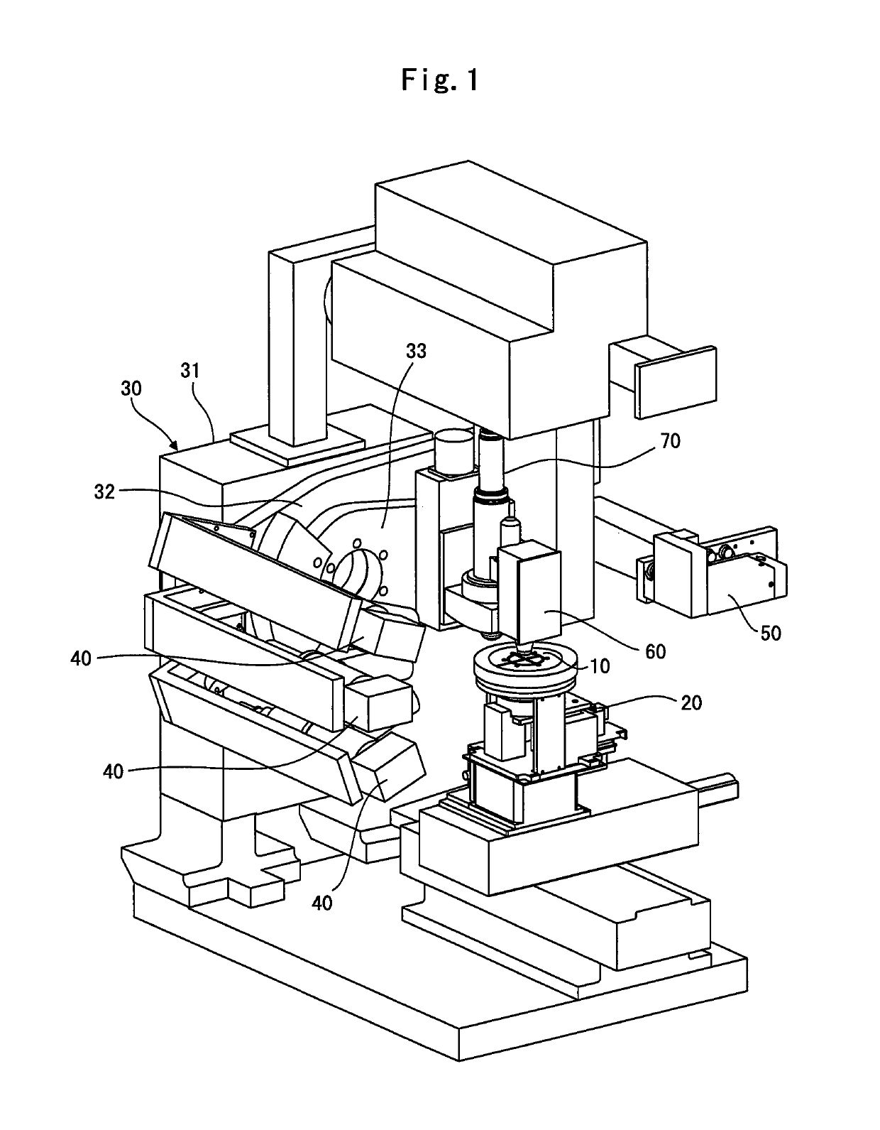
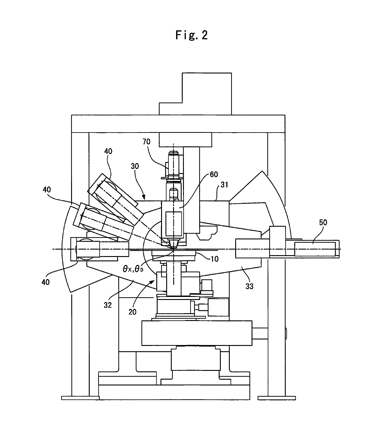
[0103]Next, a first embodiment according to the X-ray irradiation unit 40 will be described in detail with reference to FIGS. 6 to 15.

[0104]The X-ray irradiation unit 40 has an external appearance as shown in FIG. 6, and it can perform downsizing and lightening as a module configuration having an X-ray tube 42 as an X-ray source and an X-ray optical element 43 incorporated in a tube shield (unit main body) 41 as shown in FIGS. 7 and 8. The tube shield 41 is formed of a metal material for shielding X-rays, and divided into a first tube 41a containing the X-ray tube 42 therein and a second tube 41b containing the X-ray optical element 43 therein. The tubes 41a and 41b are joined and unified into one body by fastening means such as a bolt or the like.

[0105]As shown in FIG. 7, an X-ray path for leading X-rays radiated from the X-ray tube 42 to an X-ray emission port 41c is formed in the tube shield 41, and a shutter 45 for opening / closing the X-ray path is arranged in the first tube 41a...

second embodiment

[0130]Next, the X-ray irradiation unit 40 will be described in detail with reference to FIGS. 16 to 19.

[0131]The X-ray irradiation unit 40 of this embodiment is configured so as to be capable of irradiating large-intensity X-rays suitable for the fluorescence X-ray measurement.

[0132]The X-ray irradiation unit 40 has an exterior appearance as shown in FIG. 16, and designed in a module configuration that an X-ray tube 42 as an X-ray source and an X-ray optical element 43 are incorporated in a tube shield (unit main body) 41. The tube shield 41 is formed of a metal material for shielding X-rays, and divided into a first tube 41a containing the X-ray tube 42, and a second tube 41b containing the X-ray optical element 43. The respective tubes 41a and 41b are joined to each other through a joint member 41d.

[0133]As shown in FIGS. 16B and 17, an X-ray path for leading X-rays radiated from the X-ray tube 42 to an X-ray emission port 41c is formed in the tube shield 41, and a shutter 45 for...


PUM

PropertyMeasurementUnit
angleaaaaaaaaaa
spreading angleaaaaaaaaaa

Abstract

An X-ray thin film inspection device of the present invention includes an X-ray irradiation unit 40 installed on a first rotation arm 32, an X-ray detector 50 installed on a second rotation arm 33, and a fluorescence X-ray detector 60 for detecting fluorescence X-rays generated from an inspection target upon irradiation of X-rays. The X-ray irradiation unit 40 includes an X-ray optical element 43 comprising a confocal mirror for receiving X-rays radiated from an X-ray tube 42, reflects plural focused X-ray beams monochromatized at a specific wavelength and focuses the plural focused X-ray beams to a preset focal point, and a slit mechanism 46 for passing therethrough any number of focused X-ray beams out of the plural focused X-ray beams reflected from the X-ray optical element 43.

Description

TECHNICAL FIELD[0001]The present invention relates to an X-ray thin film inspection device suitable for use in a semiconductor manufacturing field, etc., such as a technical field for manufacturing an element having a multilayer structure in which many thin films are laminated on a substrate.BACKGROUND ART[0002]The characteristics of a semiconductor, etc., such as an element having a multilayer structure in which many thin films are laminated on a substrate, vary according to the state of a film to be formed, such as the film thickness, density, crystalline, etc. of the film. Microfabrication and integration of these elements have recently progressed, and this tendency has become remarkable. Therefore, a thin film inspection device that is capable of accurately measuring the states of formed films have been required.[0003]As this type of inspection device have been known direct measurement based on a cross-section transmission electron microscope (TEM), a film thickness inspection d...

Claims


Application Information

Patent Timeline
Patent Type & Authority Patents(United States)
IPC IPC(8): H05G1/02G01N23/20A61B6/08G01N23/223G01N23/2206G01N23/203G01N23/2204
CPCG01N23/2204G01N23/223G01N23/203G01N23/2206G01N2223/076G01N2223/61G01N2223/315G01N2223/6116G01N23/20
Inventor OGATA, KIYOSHIYOSHIHARA, SEIKINEFUCHI, TAKAOUMEGAKI, SHIROASANO, SHIGEMATSUHORADA, KATSUTAKAYOSHIDA, MUNEOMOTONO, HIROSHITAKAHASHI, HIDEAKIHIGUCHI, AKIFUSAOMOTE, KAZUHIKOITO, YOSHIYASUKAWAHARA, NAOKINAKANO, ASAO
Owner RIGAKU CORP
Why Eureka
Try Eureka