Designed waveform generator for semiconductor equipment, plasma processing apparatus, method of controlling plasma processing apparatus, and method of manufacturing semiconductor device

a waveform generator and semiconductor technology, applied in pulse train generators, instruments, generating/distributing signals, etc., can solve problems such as difficulty in precise control of plasma reactions

Active Publication Date: 2019-11-12
SAMSUNG ELECTRONICS CO LTD
View PDF13 Cites 20 Cited by
  • Summary
  • Abstract
  • Description
  • Claims
  • Application Information

AI Technical Summary

Problems solved by technology

However, it can be difficult to precisely control the plasma reaction.

Method used


Image

  • Designed waveform generator for semiconductor equipment, plasma processing apparatus, method of controlling plasma processing apparatus, and method of manufacturing semiconductor device
  • Designed waveform generator for semiconductor equipment, plasma processing apparatus, method of controlling plasma processing apparatus, and method of manufacturing semiconductor device
  • Designed waveform generator for semiconductor equipment, plasma processing apparatus, method of controlling plasma processing apparatus, and method of manufacturing semiconductor device

Examples


Embodiment Construction

[0035]Hereinafter, the present inventive concept will be explained in detail with reference to the accompanying drawings.

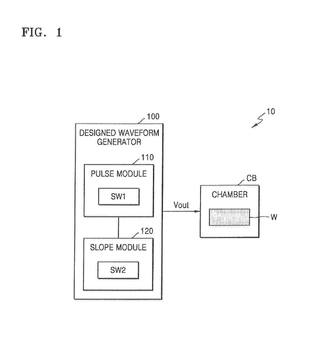
[0036]FIG. 1 is a block diagram showing semiconductor equipment 10 according to an exemplary embodiment of the inventive concept. The semiconductor equipment 10 may be used to manufacture a semiconductor.

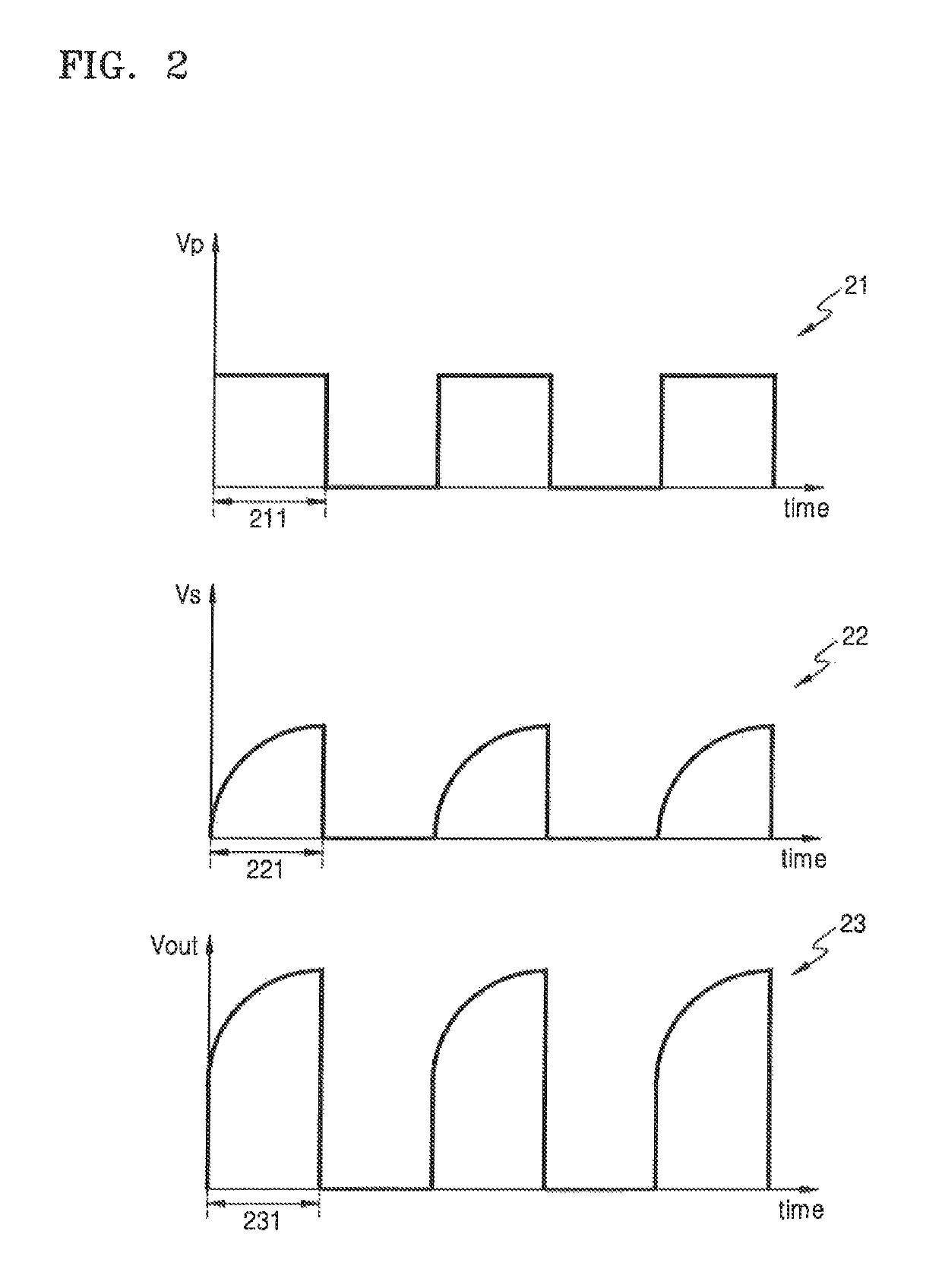
[0037]Referring to FIG. 1, the semiconductor equipment 10 includes a designed waveform generator 100 and a chamber CB. The designed waveform generator 100 generates an output voltage Vout having an arbitrary waveform (hereinafter, referred to as a “designed waveform”) designed by a user and provides the generated output voltage Vout to the chamber CB. For instance, the designed waveform may have a frequency in a range from a few kHz to a few MHz or may have a variable voltage level in a range from tens of volts (V) to several tens of kilo-volts (kV). A semiconductor wafer W is loaded in the chamber CB, and a semiconductor process is performed on the semiconductor ...


PUM


Abstract

A designed waveform generator includes at least one first signal generator including a first switching device and generating a square wave having a constant voltage level during an on-period of the first switching device and at least one second signal generator including a second switching device and controlling a transition period of the second switching device to generate a variable waveform having a variable voltage level during the transition period of the second switching device. The at least one first signal generator and the at least one second signal generator are connected to each other in a cascade manner.

Description

CROSS-REFERENCE TO RELATED APPLICATION[0001]This application claims the benefit of Korean Patent Application No. 10-2016-0094828, filed on Jul. 26, 2016, in the Korean Intellectual Property Office, the disclosure of which is incorporated herein in its entirety by reference.BACKGROUND1. Technical Field[0002]The inventive concept relates to a semiconductor equipment, and more particularly, to a designed waveform generator for a semiconductor equipment, a plasma processing apparatus, a method of controlling the plasma processing apparatus, and a method of manufacturing a semiconductor device.2. Discussion of Related Art[0003]Semiconductors are crystalline or amorphous solids with distinct electrical characteristics. Semiconductors have a resistance higher than typical resistance materials, but lower than insulators.[0004]In general, a semiconductor is manufactured using a depositing process to deposit a thin layer and an etching process to etch the thin layer. For example, the etching ...

Claims


Application Information

Patent Timeline
Patent Type & Authority Patents(United States)
IPC IPC(8): G06F1/12H02M7/49H01J37/32H03K3/02H03K3/021H03K3/64G06F1/03G06F1/06H02M3/337H03M1/00H02M1/00
CPCG06F1/12G06F1/06H02M7/49H03K3/02H03K3/64G06F1/0321H01J37/321H03K3/021Y02B70/1491H02M2001/007H02M3/337H02M2001/0058H02M2001/0045Y02B70/10H02M1/0045H02M1/0058H02M1/007H02M3/33573H01J37/32128H01J37/32165H01J2237/3321H01J2237/334
Inventor KIM, HYUN-BAESOH, SANG-YOONCHOIKIM, JIN-HO
Owner SAMSUNG ELECTRONICS CO LTD
Why Eureka
Try Eureka