
Leakage compensation read method for memory device

a memory device and leakage compensation technology, applied in the field of leakage compensation read method of memory devices, can solve the problems of reducing the sensing margin available for the array, affecting the operation of the sensing circuitry, and increasing current, so as to reduce the loss of read margin arising from leakage curren

Active Publication Date: 2019-11-12
MACRONIX INT CO LTD
View PDF13 Cites 4 Cited by
  • Summary
  • Abstract
  • Description
  • Claims
  • Application Information

AI Technical Summary

Benefits of technology

[0008]A technology is described to compensate for leakage current from unselected memory cells suitable for use in high density memory, including cross-point memory arrays. Utilizing the technology described herein, loss of read margin arising from leakage current can be reduced.
[0014]As a result of the technology described herein, high density integrated circuit memory devices with improved read margin can be achieved.

Problems solved by technology

During sensing of data from a selected memory cell, unselected memory cells coupled to the bit line can contribute leakage current that can interfere with the operation of the sensing circuitry.
As the number of unselected memory cells increases, the contributions of leakage current adds up and reduces the sensing margin available for the array.
Similar leakage current problems arise in other memory architectures, including for example NOR flash architectures.

Method used


Image

  • Leakage compensation read method for memory device
  • Leakage compensation read method for memory device
  • Leakage compensation read method for memory device

Examples


Embodiment Construction

[0022]A detailed description of embodiments of the present invention is provided with reference to the FIGS. 1-6.

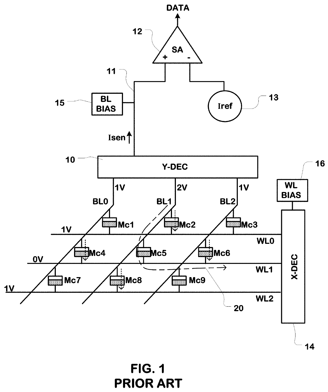
[0023]FIG. 1 illustrates a representative portion of a prior art memory array, such as a level in a 3D cross-point array. The illustrated portion of the memory array includes a plurality of memory cells, including in the illustrated example memory cells Mc1 to Mc9.

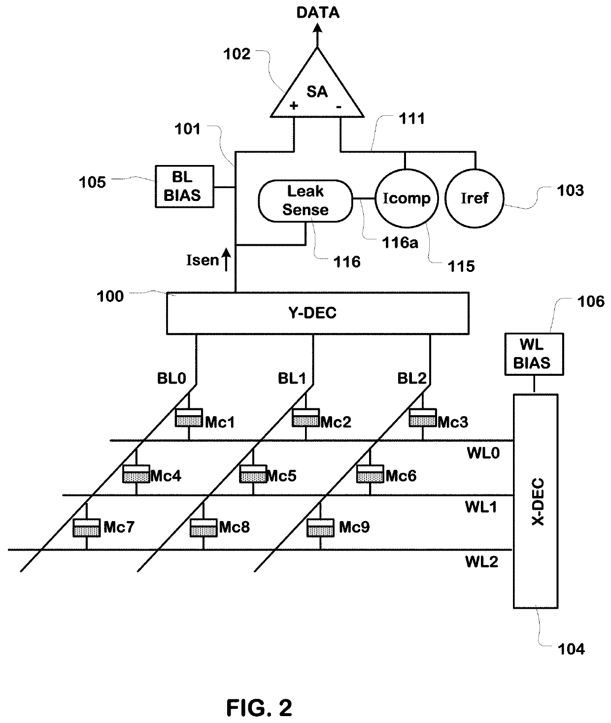
[0024]The memory array includes a plurality of bit lines, including in the illustrated example, bit lines BL0 to BL2. Likewise, the memory cell array includes a plurality of word lines, including in the illustrated example, word lines WL0 to WL2. Of course, the number of memory cells, bit lines and word lines can be much higher in practical memory devices.

[0025]The memory cells Mc1, Mc4 and Mc7 are coupled to a bit line BL0, and disposed at the cross-points of bit line BL0 with the plurality of word lines WL0 to WL2.

[0026]The memory cells Mc2, Mc5 and Mc8 are coupled to a bit line BL1, and disposed at the cross-...


PUM


Abstract

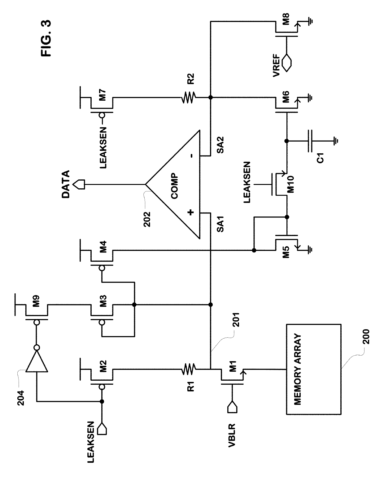
A memory device including an array of memory cells including bit lines, and biasing circuitry cells. A sense amplifier has a data line input connected to a data line, and a reference input. The controllable reference current source can be connected to the reference input of the sense amplifier. Control circuits on the device are configured to cause execution of a read operation, where the read operation includes a first phase in which the array is biased to induce leakage current on the selected bit line, and a second phase in which the array is biased to read a selected memory cell on the selected bit line. A circuit on the device is configured to sample the leakage current in the first phase, and to control the controllable reference current source during the second phase, as a function of the sampled leakage current.

Description

BACKGROUND[0001]Field[0002]The present invention relates to integrated circuit memory, and more specifically to technology for accurately sensing data stored in large-scale memory arrays.[0003]Description of Related Art[0004]The size of memory arrays in integrated circuit memory devices has been steadily increasing. As a result, a single bit line in a large-scale memory array can be coupled with a very large number of individual memory cells. During sensing of data from a selected memory cell, unselected memory cells coupled to the bit line can contribute leakage current that can interfere with the operation of the sensing circuitry. As the number of unselected memory cells increases, the contributions of leakage current adds up and reduces the sensing margin available for the array.[0005]One type of memory array in which this problem is encountered includes programmable resistance memory devices with a high density array of cells organized in a cross-point architecture, such as des...

Claims


Application Information

Patent Timeline
Patent Type & Authority Patents(United States)
IPC IPC(8): G11C13/00G11C11/16G11C27/02
CPCG11C11/1673G11C13/0033G11C13/004G11C13/0026G11C13/0038G11C2013/0054G11C27/024G11C2013/0042G11C2013/0057G11C13/0004G11C2013/0045
Inventor YANG, SHANG-CHILIAO, CHUN-YUCHEN, KEN-HUI
Owner MACRONIX INT CO LTD
Learn More