Resistive memory storage apparatus and writing method thereof including disturbance voltage

a memory storage apparatus and resistance state technology, applied in the direction of information storage, static storage, digital storage, etc., can solve the problem that the filament of the memory cell with low resistance state is robust enough to pass the high temperature data retention (htdr) and endurance tests, and achieve good high temperature data retention and endurance

Active Publication Date: 2019-11-26
WINBOND ELECTRONICS CORP
View PDF19 Cites 0 Cited by
  • Summary
  • Abstract
  • Description
  • Claims
  • Application Information

AI Technical Summary

Benefits of technology

[0005]The invention provides a resistive memory storage apparatus and a writing method thereof, and a filament thereof is robust with good high temperature data retention and good endurance.
[0008]In summary, in the exemplary embodiments of the invention, the memory controlling circuit determines to apply the second set voltage or the second disturbance voltage on the memory cell according to the magnitude relationship between the reading currents of the memory cell before / after the first disturbance voltage is applied so as to maintain the high temperature data retention of the memory storage apparatus and optimize the endurance of the memory storage apparatus.

Problems solved by technology

However, in the existing techniques, after the set operation is performed on the existing resistive memory, although a memory cell with low resistance state (LRS) can be obtained and the reading current is large, the large reading current cannot acquire whether the filament of the memory cell with low resistance state is robust enough to pass the high temperature data retention (HTDR) and endurance tests.

Method used


Image

  • Resistive memory storage apparatus and writing method thereof including disturbance voltage
  • Resistive memory storage apparatus and writing method thereof including disturbance voltage
  • Resistive memory storage apparatus and writing method thereof including disturbance voltage

Examples


Embodiment Construction

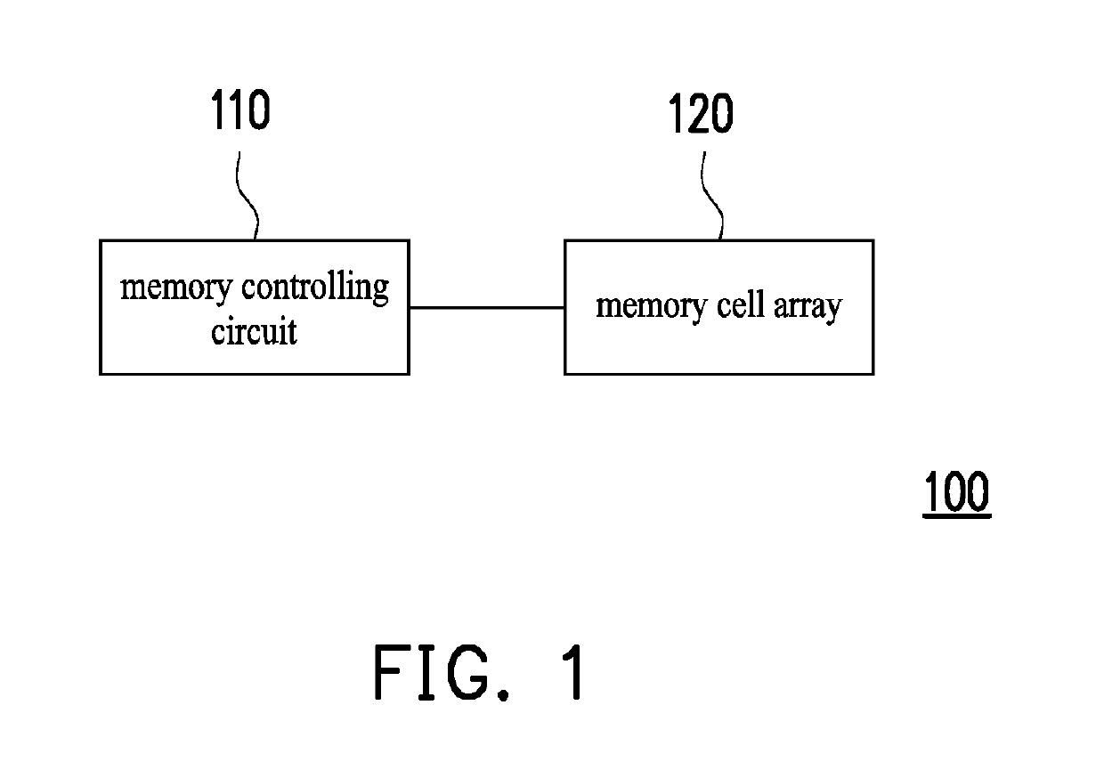
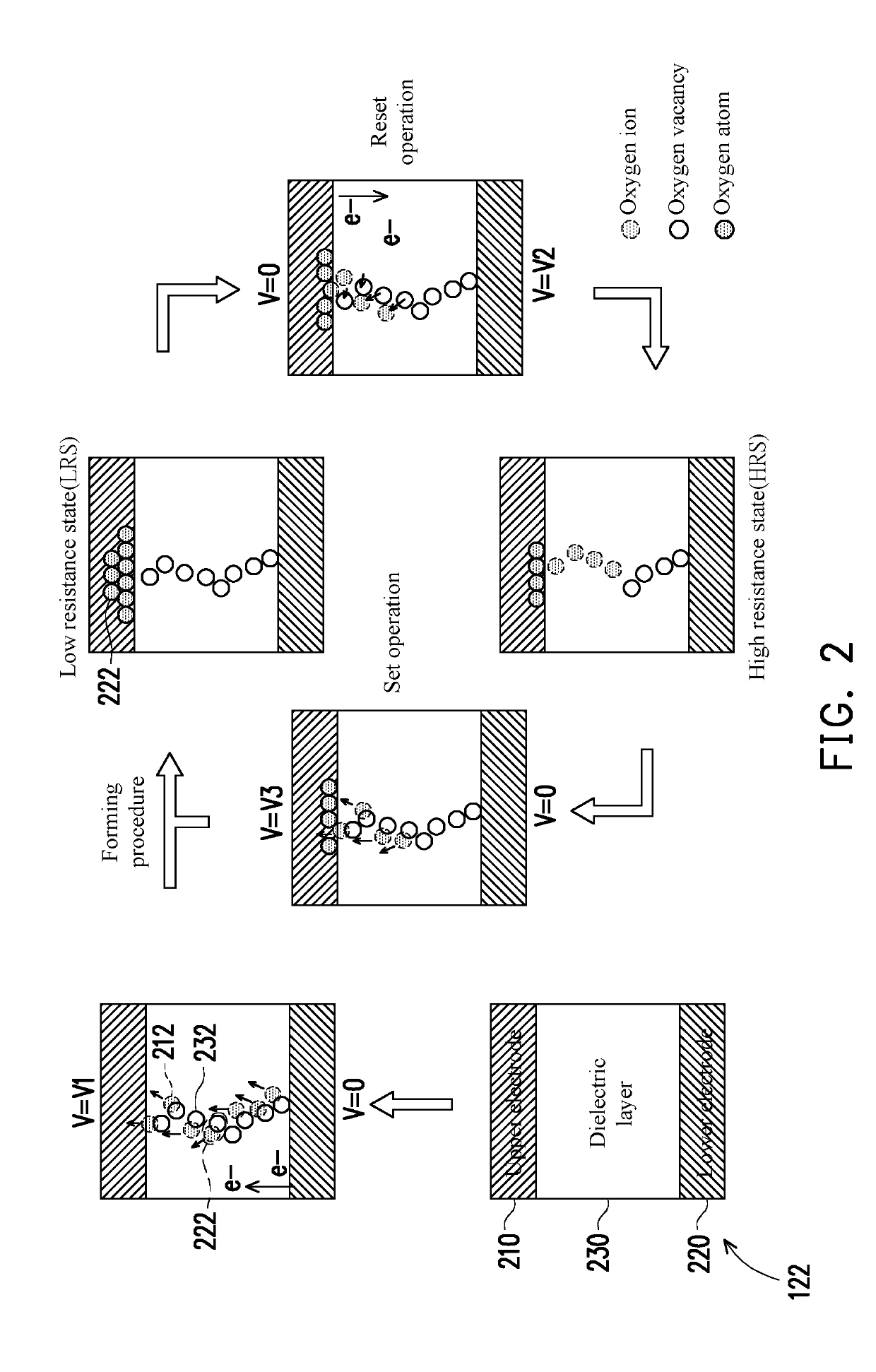
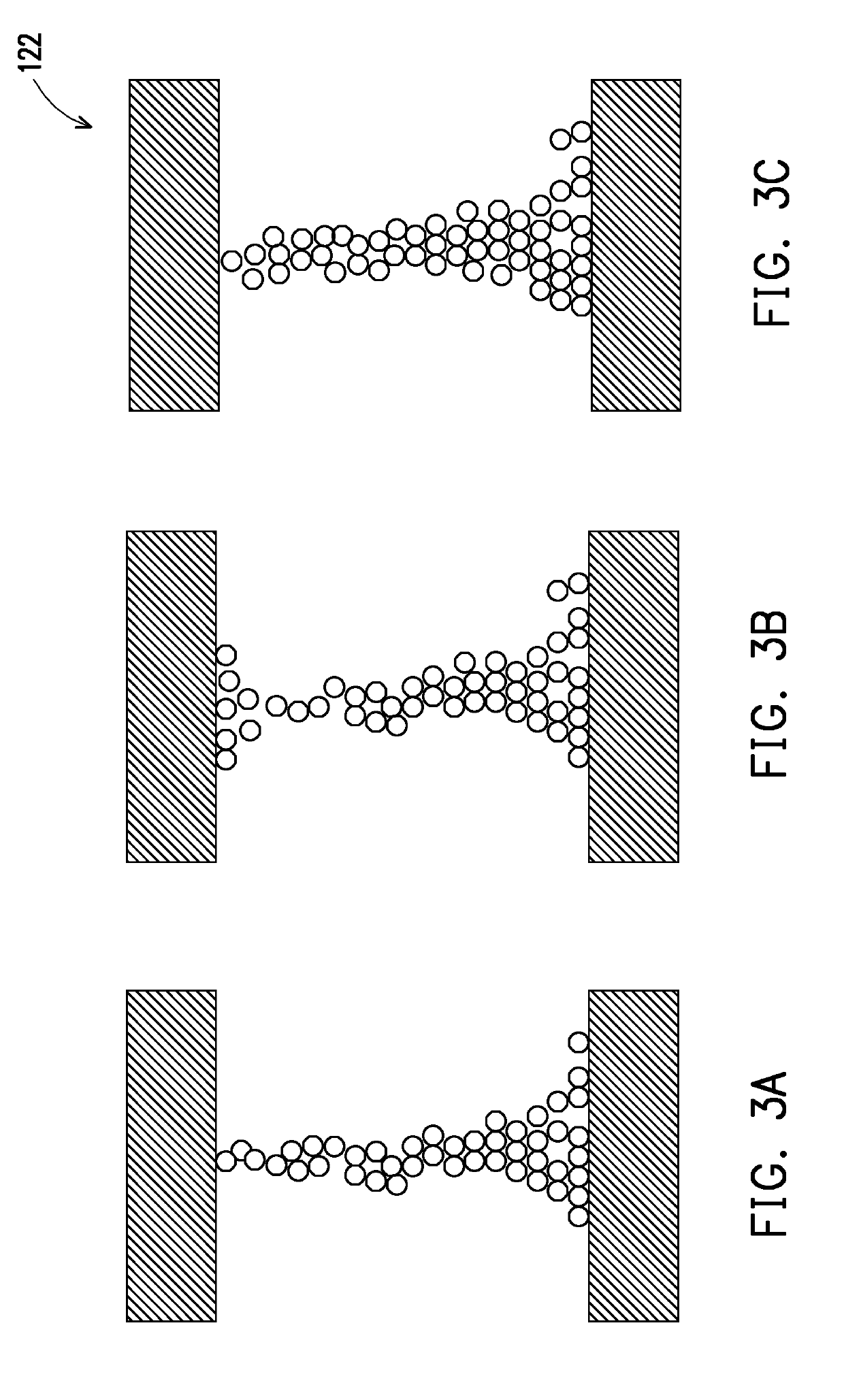
[0018]Referring to FIG. 1 and FIG. 2, a memory storage apparatus 100 in the embodiment includes a memory controller 110 and a memory cell array 120. The memory cell array 120 is coupled to the memory controller 110. The memory cell array 120 includes a plurality of memory cells 122 arranged in arrays. In the embodiment, a resistive memory device 122 includes an upper electrode 210, a lower electrode 220 and a dielectric layer 230 disposed between the upper electrode 210 and the lower electrode 220. The dielectric layer 230 includes a dielectric material such as a transition metal oxide (TMO). The memory cell 122 with such structure at least has two resistance states. The resistance state of the resistive memory device 122 is changed by applying different voltages on both ends of the electrode so as to provide the function of storing data.

[0019]In the embodiment, the memory controller 110 is used to perform a forming procedure on the memory cell 122. The forming procedure refers to a...


PUM


Abstract

A writing method of a resistive memory storage apparatus is provided. The writing method includes: applying a first set voltage on a memory cell, and acquiring a first reading current of the memory cell; applying a first disturbance voltage on the memory cell, and acquiring a second reading current of the memory cell; and determining to apply a second set voltage or a second disturbance voltage on the memory cell according to a magnitude relationship between the first reading current and the second reading current. An absolute value of the first disturbance voltage is smaller than an absolute value of a reset voltage, and an absolute value of the second disturbance voltage is smaller than an absolute value of the second set voltage. In addition, a resistive memory storage apparatus is also provided.

Description

CROSS-REFERENCE TO RELATED APPLICATION[0001]This application claims the priority benefit of China application serial no. 201710700423.8, filed on Aug. 16, 2017. The entirety of the above-mentioned patent application is hereby incorporated by reference herein and made a part of this specification.TECHNICAL FIELD[0002]The invention is related to a memory storage apparatus and a writing method thereof, and particularly to a resistive memory storage apparatus and a writing method thereof.DESCRIPTION OF RELATED ART[0003]Existing resistive memories normally include an upper electrode and a lower electrode configured to be opposite to each other and a dielectric layer disposed between the upper electrode and the lower electrode. When performing a set operation on the existing resistive memory, it is required to perform a filament forming procedure first by applying a positive bias to the resistive memory so that the current flows from the upper electrode to the lower electrode and an oxyge...

Claims


Application Information

Patent Timeline
Patent Type & Authority Patents(United States)
IPC IPC(8): G11C13/00
CPCG11C13/0069G11C13/0064G11C13/0097G11C13/0007G11C2013/009G11C2013/0076G11C13/0002G11C13/0033G11C13/004G11C2013/0083
Inventor LIN, LIH-WEICHENG, JU-CHIEHTSAI, TSUNG-HUANTSENG, I-HSIEN
Owner WINBOND ELECTRONICS CORP
Why Eureka
Try Eureka