Method for manufacturing semiconductor device

a semiconductor and manufacturing technology, applied in the direction of film/foil adhesives, non-macromolecular adhesive additives, adhesive types, etc., can solve the problem of insufficient antistatic property, achieve excellent quality, stably obtained, and achieve excellent antistatic properties

Active Publication Date: 2019-12-24
MITSUI CHEM TOHCELLO INC
View PDF19 Cites 1 Cited by
  • Summary
  • Abstract
  • Description
  • Claims
  • Application Information

AI Technical Summary

Benefits of technology

[0055]According to the present invention, it is possible to provide a method for manufacturing a semiconductor device in which the grinding of a semiconductor wafer can be stably carried out, the insulation breakdown of a circuit can be suppressed, and a semiconductor device having an excellent quality can be stably obtained.

Problems solved by technology

According to the present inventors' studies, it has been clarified that, in an adhesive film having a base material film, an antistatic layer, and an adhesive layer laminated in this order as described in Patent Document 1, the antistatic property is not sufficiently satisfactory.

Method used


Image

  • Method for manufacturing semiconductor device

Examples


example 1

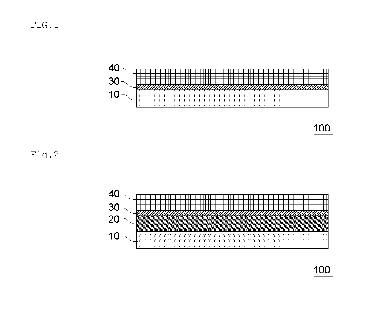
[0224]An unevenness-absorbing resin 1 which served as the unevenness-absorbing resin layer was extrusion-laminated on a polyethylene terephthalate which served as the base material layer in a thickness of 195 μm, thereby obtaining a bilayer laminate film.

[0225]Next, the material for forming the antistatic layer 1 was applied onto and dried on a separately-prepared mold-release film to form an antistatic film, and this antistatic film was laminated on the unevenness-absorbing resin layer, thereby forming a 0.1 μm-thick antistatic layer.

[0226]Next, the coating fluid for an adhesive resin layer 1 was applied and then dried on the antistatic layer of the obtained laminate film, thereby forming a 40 μm-thick adhesive resin layer and thus obtaining an adhesive film.

[0227]The following evaluations were carried out on the obtained adhesive film. The obtained results are shown in Table 1.


PUM

PropertyMeasurementUnit
thicknessaaaaaaaaaa
thicknessaaaaaaaaaa
electrostatic potential V1aaaaaaaaaa

Abstract

A method for manufacturing a semiconductor device includes at least the following three steps. A step (A) of preparing a structure including a semiconductor wafer having a circuit-formed surface and an adhesive film attached to the circuit-formed surface side of the semiconductor wafer. A step (B) of back grinding a surface on a side opposite to the circuit-formed surface side of the semiconductor wafer. A step (C) of radiating ultraviolet rays to the adhesive film and then removing the adhesive film from the semiconductor wafer. In addition, as the adhesive film, an adhesive film having a base material layer, an antistatic layer, and an adhesive resin layer including a conductive additive in this order is used, and the adhesive film is used so that the adhesive resin layer faces the circuit-formed surface side of the semiconductor wafer.

Description

TECHNICAL FIELD[0001]The present invention relates to a method for manufacturing a semiconductor device.BACKGROUND ART[0002]Among steps for manufacturing a semiconductor device, in a step of grinding a semiconductor wafer, an adhesive film is attached to the semiconductor wafer in order to prevent damage of the semiconductor wafer.[0003]As the above-described adhesive film, generally, a film obtained by laminating an ultraviolet-curable adhesive resin layer on a base material film is used. When this adhesive film is irradiated with ultraviolet rays, the adhesive resin layer cross-links, and the adhesive force of the adhesive resin layer decreases, and thus the adhesive film can be easily peeled off from the semiconductor wafer.[0004]Meanwhile, in steps for manufacturing a semiconductor device using the above-described adhesive film, there have been cases in which static electricity called peeling charging is generated during the peeling of the adhesive film from the semiconductor wa...

Claims


Application Information

Patent Timeline
Patent Type & Authority Patents(United States)
IPC IPC(8): H01L21/68C09J9/02H01L21/683H01L23/00C09J133/08H01L21/306
CPCH01L21/30625H01L21/6835C09J9/02C09J133/08H01L24/13H01L2924/014H01L2224/13147C09J199/00H01L2224/13101H01L24/11H01L2224/11001H01L21/6836H01L2221/6834H01L2221/68381H01L2221/68327C09J7/29C09J2203/326C08K2201/001C09J2301/408C09J2301/416H01L2924/00014C09J7/20C09J11/02H01L21/304H01L21/67132C09J2301/312
Inventor KURIHARA, HIROYOSHI
Owner MITSUI CHEM TOHCELLO INC
Why Eureka
Try Eureka