Semiconductor device and method of operating thereof

a technology of semiconductor devices and semiconductors, applied in the field of semiconductor devices, can solve the problems of affecting the stability of the operation, the operating rate of the sense amplifier b>106/b> is lowered, and the embedded dram read is difficult to read, so as to reduce power consumption, stably carry out the read operation, and reduce the power source voltage

Active Publication Date: 2011-10-04
RENESAS ELECTRONICS CORP
View PDF3 Cites 0 Cited by
  • Summary
  • Abstract
  • Description
  • Claims
  • Application Information

AI Technical Summary

Benefits of technology

[0013]The present invention provides a semiconductor device having a memory circuit, which enables to reduce power consumption. Further, the semiconductor device having the memory circuit makes it possible to stably carry out the read operation while lowering a power source voltage.

Problems solved by technology

However, as lowering of a power source voltage progresses, a threshold voltage of an MOS transistor comes close to a power source voltage, so that there is a possibility that a fast read of the embedded DRAM is difficult.
In this case, if the VDD is lowered, (VDD−ΔV) approaches to Vth, and this causes a danger that an operating rate of the sense amplifier 106 is lowered.
In addition, if the VDD is lowered, the influence of ΔV is increased and it is danger that variation of ΔV influences stability of the operation, because ΔV is changed due to variation of Cb / Cs that is easily influenced by the production tolerance.

Method used


Image

  • Semiconductor device and method of operating thereof
  • Semiconductor device and method of operating thereof
  • Semiconductor device and method of operating thereof

Examples


first embodiment

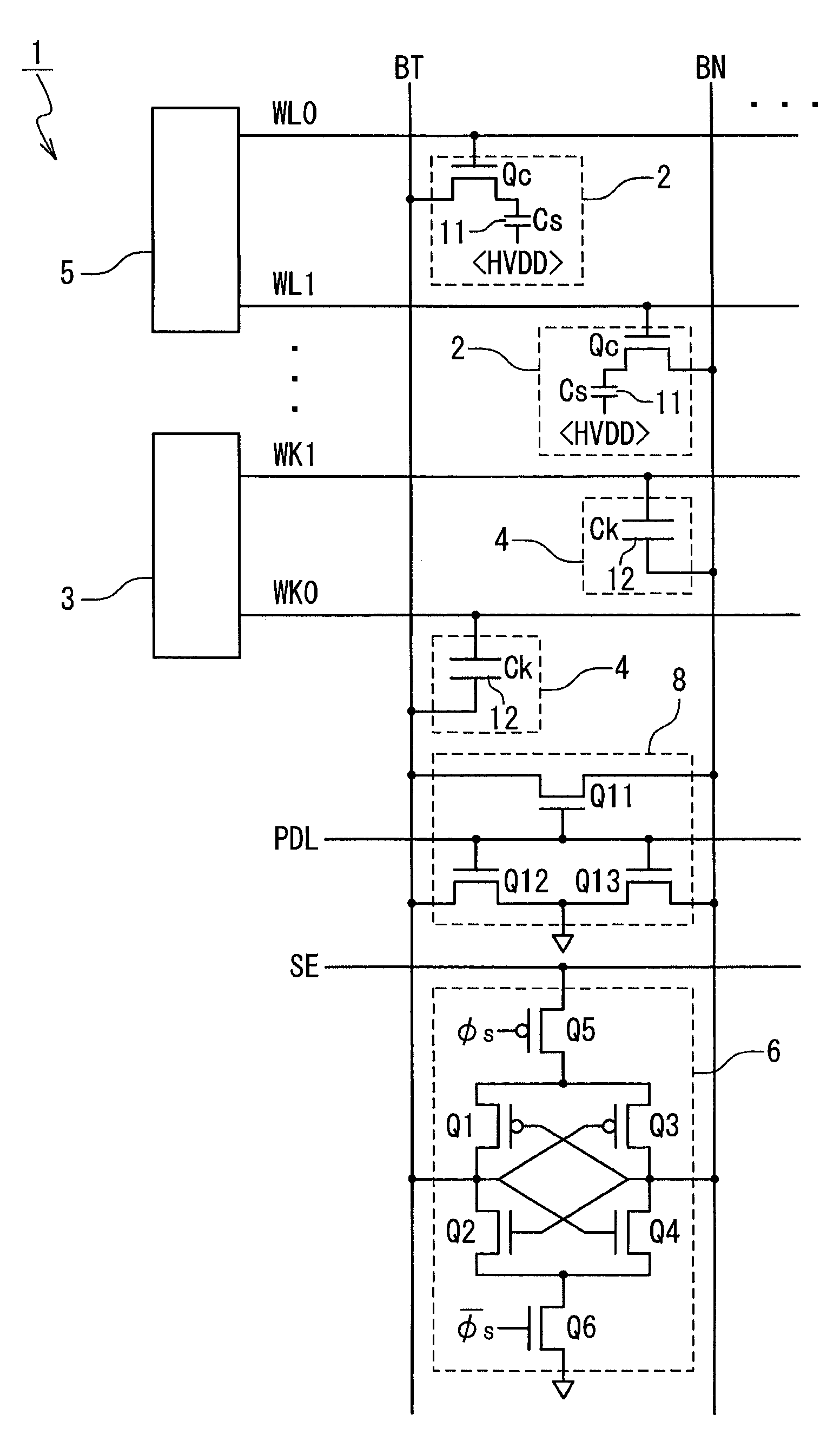
[0026]FIG. 3 is a circuit diagram showing a configuration of a semiconductor device according to a first embodiment of the present invention. This semiconductor device 1 includes a memory cell 2, a word line decoder 5, a precharge circuit 8, a potential generating circuit 3, a negative kicker circuit 4, and a sense amplifier 6. Here, representing the bit lines, only a pair of bit lines will be described with the illustration of this pair.

[0027]The memory cell 2 is connected to any one of a first bit line BT and a second bit line BN to store a data. The memory cell 2 includes a cell capacitor 11 and a cell transistor Qc. The cell capacitor 11 serves as a capacitor of a capacitance Cs to accumulate electric charges corresponding to the data, and has one terminal, which is connected to a power source of a HVDD (½·VDD). The cell transistor Qc includes a gate and source / drain regions. The gate is connected to a first word line WL (WL0, WL1, . . . ) for selecting the memory cell 2. One of...

second embodiment

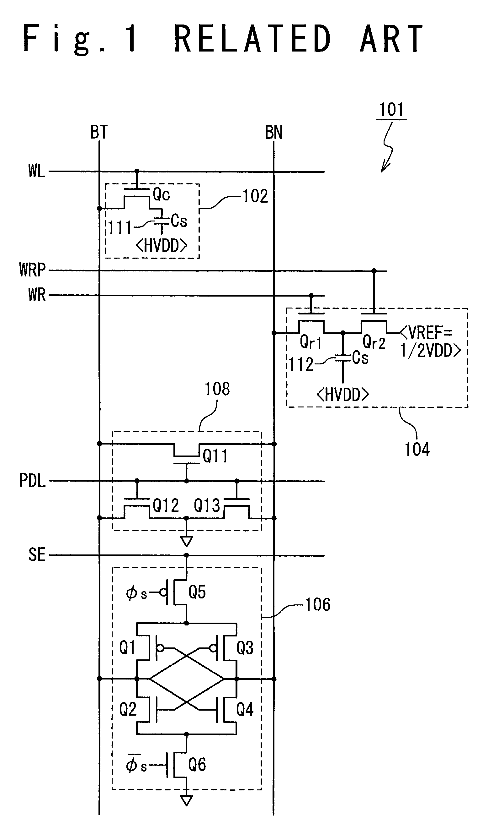
[0048]FIG. 7 is a circuit diagram showing a configuration of a semiconductor device according to a second embodiment of the present invention. This semiconductor device 1 includes a memory cell 2, a word line decoder 5, a precharge circuit 8, a potential generating circuit 3, a negative kicker circuit 4, and a sense amplifier 6. According to the present embodiment, a basic configuration is the same as the first embodiment (FIG. 3). However, detailed configurations of the potential generating circuit 3 and the negative kicker circuit 4 are different from those of the first embodiment.

[0049]In other words, the capacitance Ck of the negative potential capacitor 12 of the negative kicker circuit 4 is determined to be approximately equal to the capacitance Cs of the cell capacitor 11 (Ck=Cs). In this case, the potential generating circuit 3 applies a potential, which is half (VDD / 2) of the power source voltage VDD to be supplied to the sense amplifier 6, to the negative potential capacit...


PUM


Abstract

A semiconductor device includes: a memory cell; a precharge circuit; a negative potential applying circuit; and a sense amplifier. The memory cell is connected to a first bit line and store data. The precharge circuit is connected to the first and second bit lines and precharges the first and second bit lines to a ground potential. The negative potential applying circuit is connected to the first bit line and applies a negative potential to the first bit line. The sense amplifier is connected to the first and second bit lines and read data based on a difference between a first potential of the first bit line and a second potential of the second bit line. An absolute value of the negative potential is smaller than the difference between the first potential and the second potential.

Description

INCORPORATION BY REFERENCE[0001]This application is based upon and claims the benefit of priority from Japanese patent application No. 2008-266679 filed on Oct. 15, 2008, the disclosure of which is incorporated herein in its entirety by reference.BACKGROUND OF THE INVENTION[0002]1. Field of the Invention[0003]The present invention relates to a semiconductor device and a method of operating thereof, and particularly, the present invention relates to a semiconductor device having a circuit, which is used for a memory, and a method of operating thereof.[0004]2. Description of Related Art[0005]A semiconductor integrated circuit having a memory such as a dynamic random access memory (DRAM) integrated therein has been known. In recent years, in response to the demand of low power consumption, a semiconductor integrated circuit is progressing in lowering of a power source voltage. In response to the demands of this, an embedded DRAM also is progressing in lowering of a power source voltage...

Claims


Application Information

Patent Timeline
Patent Type & Authority Patents(United States)
IPC IPC(8): G11C11/24
CPCG11C7/12G11C8/10G11C11/4074G11C11/4094
Inventor TAKAHASHI, HIROYUKI
Owner RENESAS ELECTRONICS CORP
Why Eureka
Try Eureka