Semiconductor differential pressure sensor and manufacturing method of the same

a technology of differential pressure sensor and semiconductor, applied in the direction of fluid pressure measurement, fluid pressure measurement by electric/magnetic elements, instruments, etc., can solve the problems of thermal strain measurement error, insufficient simply applying die bonding material to the lower surface side of the sensor chip, and difficulty in obtaining the desired function, etc., to achieve high reliability, high precision measurement, and stable carry

Active Publication Date: 2018-05-03
MITSUBISHI ELECTRIC CORP
View PDF1 Cites 0 Cited by
  • Summary
  • Abstract
  • Description
  • Claims
  • Application Information

AI Technical Summary

Benefits of technology

[0018]The invention, having been contrived to solve the heretofore described kinds of problems, has for an object to obtain a highly reliable semiconductor differential pressure sensor which can stably carry out a high precision measurement in as wid

Problems solved by technology

A filter, such as a diesel particulate filter (DPF) or a gasoline particulate filter (GPF), is used in this kind of system so as to prevent particulates from being exhausted to the external environment, but in either case, the filter clogs as a result of an increase in the use thereof, leading to a difficulty in obtaining its desired function.
Because of this, it is insufficient simply to apply a die bond material to the lower surface side of the sensor chip, and measures are taken to thickly apply a die bond material also to the side surface of the sensor chip.
On the other hand, there is the problem that as the strain sensitive elements cannot distinguish between a strain caused by a pressure difference, which should originally be measured, and a strain caused by the thermal strain of the case, a measurement error due to the thermal strain occurs.
The first problem is that in a step of forming the second depressed portion in the first substrate by etching, it is very difficult to apply resist uniformly to the portion in which the first depressed portion is already formed.
When further forming the second depressed portion in the bottom surface of the first depressed portion having this kind of depth, it is necessary to carry out masking, but severe unevenness occurs in the film thickness of resist when using a common spin coating.
Also, it is also difficult to photoengrave the pattern of the second depressed portion with high precision by focusing on the bottom surface of the first depressed portion.
Even in the event of technologically enabling these steps by taking some measures, they are costly exclusive steps.
As the second problem, there is the problem that after the second substrate and the first substrate in which are formed the first depressed portion and second depressed portion are bonded together, the diaphragm is b

Method used


Image

  • Semiconductor differential pressure sensor and manufacturing method of the same
  • Semiconductor differential pressure sensor and manufacturing method of the same
  • Semiconductor differential pressure sensor and manufacturing method of the same

Examples


first embodiment

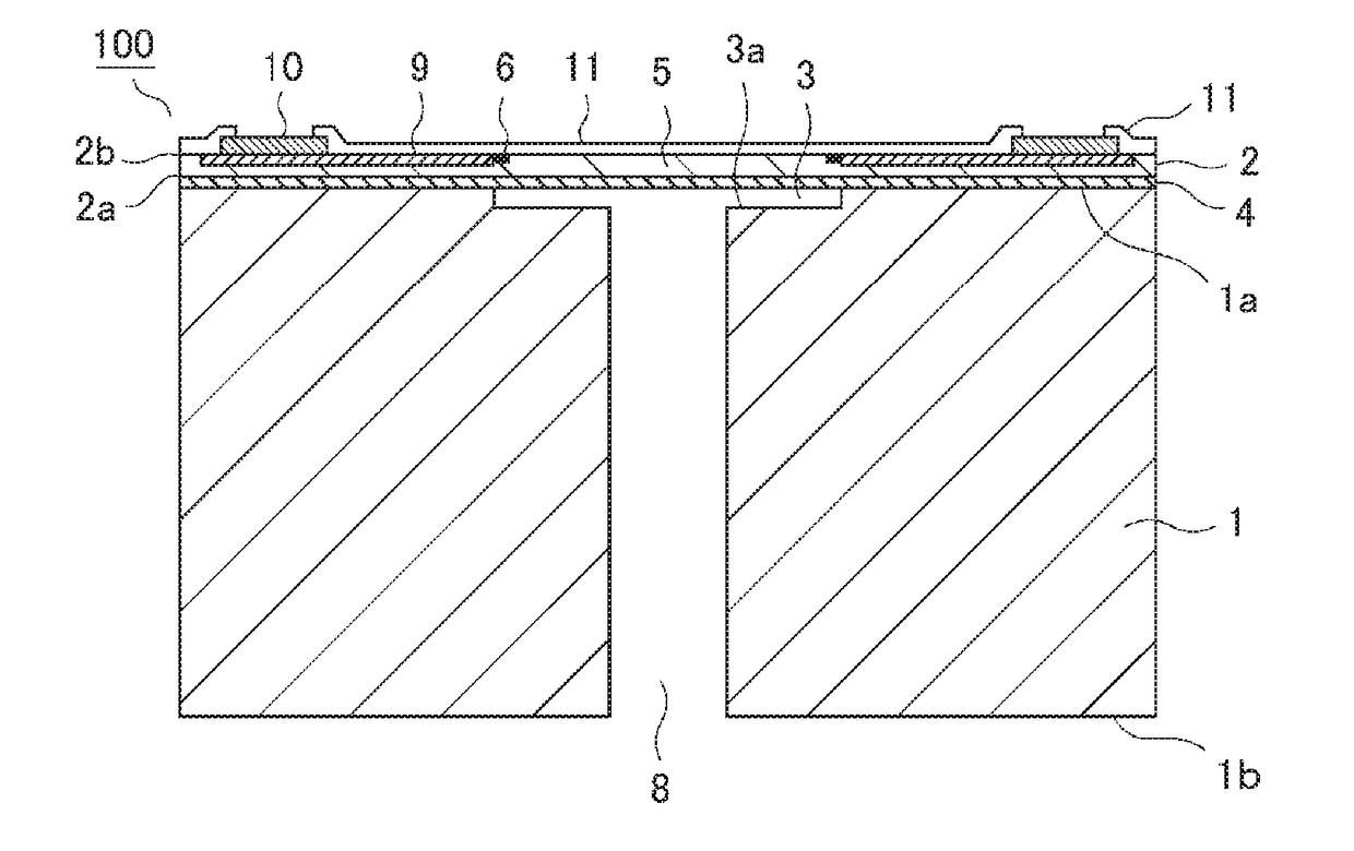
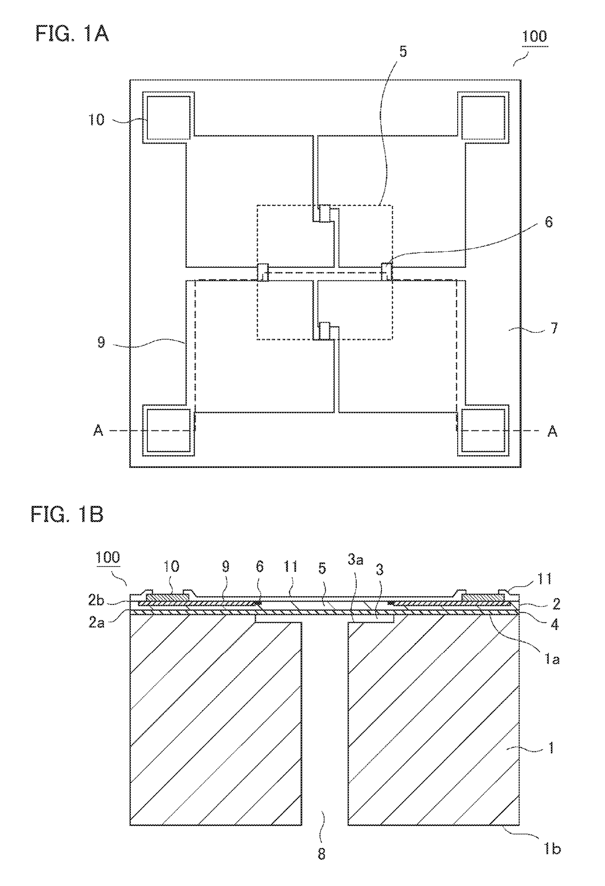
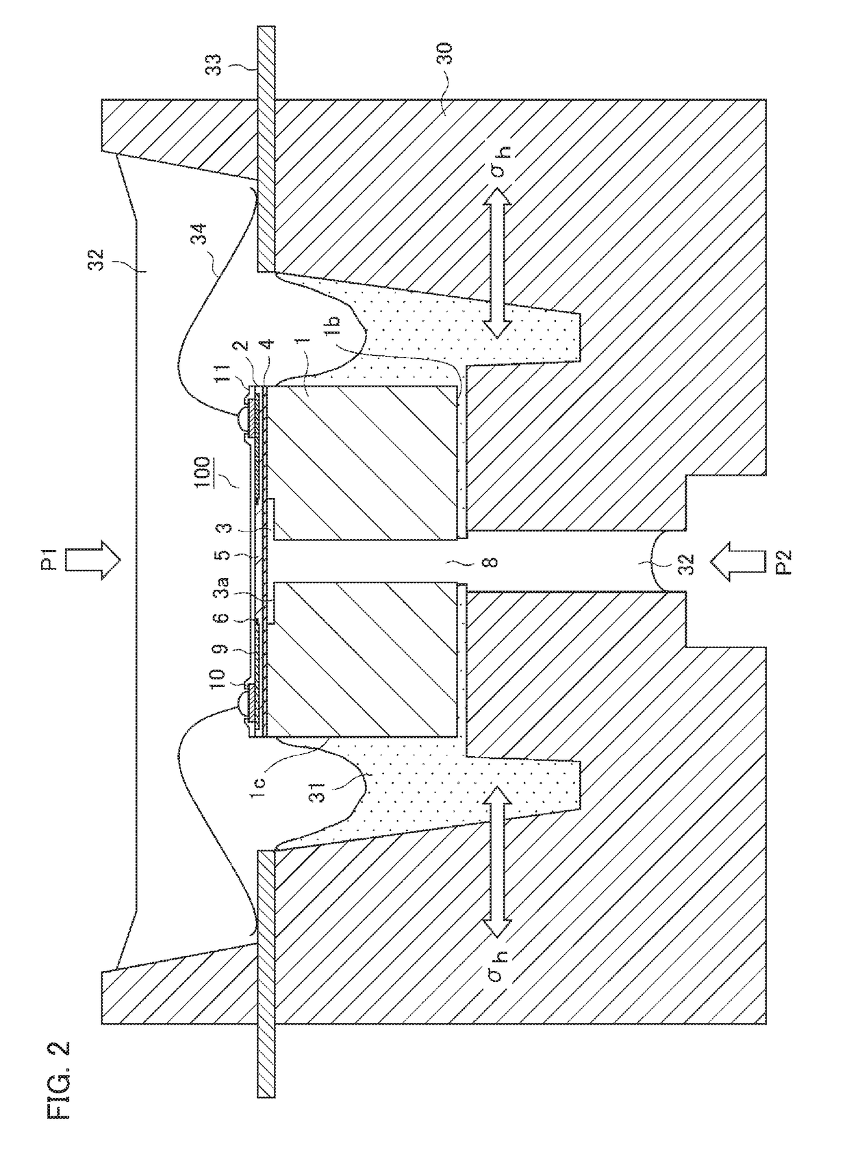
[0046]Hereafter, a description will be given, based on the drawings, of a semiconductor differential pressure sensor according to a first embodiment of the invention. FIG. 1A is a plan view showing the semiconductor differential pressure sensor according to the first embodiment, FIG. 1B is a sectional view of the portion shown by A-A in FIG. 1A, and FIG. 2 is a sectional view showing an assembly structure of the semiconductor differential pressure sensor according to the first embodiment. In the individual drawings, identical and equivalent portions are given identical signs.

[0047]The semiconductor differential pressure sensor according to the first embodiment includes a semiconductor differential pressure sensor element 100 wherein one main surface 1a of a first semiconductor substrate 1 and one main surface 2a of a second semiconductor substrate 2 are bonded together via an oxide film 4. The first semiconductor substrate 1 has a depressed portion 3 provided in the main surface 1a ...

second embodiment

[0071]FIG. 7A is a plan view showing a semiconductor differential pressure sensor element according to a second embodiment of the invention, and FIG. 7B is a sectional view of the portion shown by C-C in FIG. 7A. As the assembly structure of a semiconductor differential pressure sensor according to the second embodiment is the same as in the first embodiment, FIG. 2 is used. A semiconductor differential pressure sensor element 100A according to the second embodiment has stress relaxation grooves 13 which are disposed, in the vicinity of the strain sensitive elements 6, along the shape of the diaphragm 5. As other configurations are the same as in the first embodiment, a description will be omitted.

[0072]The stress relaxation grooves 13 are provided around and along the depressed portion 3 of the one main surface 1a of the first semiconductor substrate 1. In this way, by providing the stress relaxation grooves 13 along the boundary of the diaphragm 5, the thermal stress caused by exp...

third embodiment

[0076]FIG. 9 shows an assembly structure of a semiconductor differential pressure sensor according to a third embodiment of the invention. A semiconductor differential pressure sensor element 100C according to the third embodiment, as well as having an overhanging portion 14, which is a stepped portion, on the side surface 1c of the first semiconductor substrate 1, has minute trough-crest shaped regions 15 and 15a on the side surface 1c and main surface 1b. As other configurations are the same as in the first embodiment, a description will be omitted.

[0077]In a semiconductor differential pressure sensor, in order to ensure the hermetic separation between the front and rear thereof, a die bond material is thickly applied to not only the rear surface, but also the side surface, of a semiconductor differential pressure sensor element. Because of this, in a heretofore known semiconductor differential pressure sensor manufacturing method, there is the problem that variation occurs in the...


PUM

PropertyMeasurementUnit
Pressureaaaaaaaaaa
Areaaaaaaaaaaa
Stress relaxationaaaaaaaaaa

Abstract

A semiconductor differential pressure sensor element is such that as strain sensitive elements are disposed only inside a diaphragm, and strain relaxation grooves are provided along the diaphragm, it is difficult for thermal stress caused by expansion or contraction of a case to propagate to the strain sensitive elements, thus suppressing characteristic fluctuations resulting from a change in external temperature. Also, as a configuration is such that a sacrificial column is provided inside a depressed portion, and that the diaphragm is held by the sacrificial column in a diaphragm formation step which thins a second semiconductor substrate and a functional element formation step which repeatedly implements a cleaning step, breakage of the diaphragm can be prevented, thus achieving a significant improvement in yield.

Description

BACKGROUND OF THE INVENTIONField of the Invention[0001]The present invention relates to a semiconductor differential pressure sensor, which detects the difference between the pressures applied to the front surface and rear surface of a diaphragm, and to a manufacturing method of the sensor.Description of the Background Art[0002]In recent years, in a mode of transportation, such as a car, the regulations on exhaust gas have been reinforced from the viewpoint of environmental protection. The motorization of a power train is progressing, while a system in which is mounted a heretofore known internal combustion engine is also being improved, and there are an increasing number of cases in which an exhaust gas purification system is mounted in each of a diesel engine and gasoline engine.[0003]A filter, such as a diesel particulate filter (DPF) or a gasoline particulate filter (GPF), is used in this kind of system so as to prevent particulates from being exhausted to the external environme...

Claims


Application Information

Patent Timeline
IPC IPC(8): G01L9/00B81B3/00B81C1/00G01L19/04
CPCG01L9/0054B81B3/0072B81C1/00666B81B2203/0127G01L9/0047B81B2201/0264G01L19/04B81B7/0019B81C2201/056G01L19/0618
Inventor YOSHIKAWA, EIJI
Owner MITSUBISHI ELECTRIC CORP
Why Eureka
Try Eureka