Method for producing wired circuit board

a wired circuit board and wire technology, applied in the direction of photomechanical equipment, photosensitive material processing, instruments, etc., can solve the problem of not being able to prevent short circuit between wire patterns, and achieve the effect of preventing short circuit and preventing production of the short circuit portion caused by the above-described light focus

Active Publication Date: 2019-12-31
NITTO DENKO CORP
View PDF4 Cites 0 Cited by
  • Summary
  • Abstract
  • Description
  • Claims
  • Application Information

AI Technical Summary

Benefits of technology

[0008]An object of the present invention is to provide a method for producing a wired circuit board, in which a first wiring and a second wiring are provided highly freely and short circuit between them can be prevented.
[0020]However, with the production method of the present invention (1), the second exposure portion has an avoidance portion that avoids the bending portion when viewed from the top. In the step 4, the photoresist is exposed to light through a photomask so as to shield the photoresist corresponding to the inclined face from light, and therefore no reflected light such as the one shown in FIG. 16A is produced, i.e., the light reflected at the metal thin film corresponding to the bending portion. Therefore, in the step 5, production of the portion (assumedly removed portion) caused by the above-described light focus can be prevented. As a result, generation of the short circuit portion caused by the above-described light focus can be prevented. As a result, the short circuit between the first wiring and the second wiring can be prevented.
[0021]Furthermore, with the method of the present invention (1), the second wiring can be provided highly freely as long as the second exposure portion includes the avoidance portion and the overlapping portion.
[0033]However, with the method of the present invention (2), the second exposure portion has an avoidance portion that avoids the bending portion when viewed from the top. In the step 4, the photoresist is exposed to light through the photomask so as to shield the photoresist corresponding to the inclined face from light, and therefore reflected light reflected at the conductor layer corresponding to the bending portion as shown in FIG. 18A is not produced. Therefore, production of the short circuit portion caused by the above-described light focus can be prevented. As a result, the short circuit between the first wiring and the second wiring can be prevented.
[0034]With the production method of the present invention (2), the second wiring can be provided highly freely as long as the second exposure portion includes the avoidance portion and the overlapping portion.
[0035]With the method for producing a wired circuit board of the present invention, the first wiring and the second wiring can be provided highly freely, and their short circuit can be prevented.

Problems solved by technology

The short circuit between the wiring patterns may not be prevented.

Method used


Image

  • Method for producing wired circuit board
  • Method for producing wired circuit board
  • Method for producing wired circuit board

Examples


first embodiment

Modified Example of First Embodiment

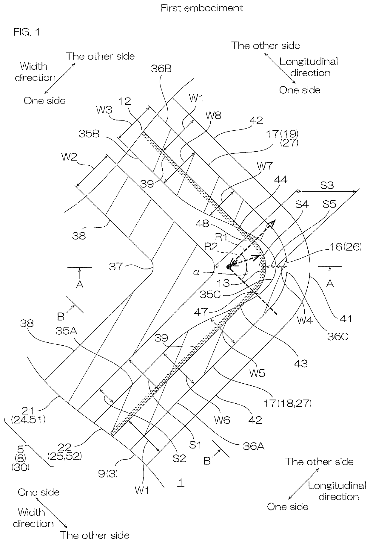
[0234]In the first embodiment, as shown in FIG. 1, two inclined face overlapping portions 17 overlap with the two insulating inclined face linear portions 39 along the entire longitudinal direction when viewed from the top.

[0235]However, the two inclined face overlapping portions 17 overlapping with the two insulating inclined face linear portions 39 partially in longitudinal direction when viewed from the top will suffice. For example, although not shown, the inclined face overlapping portion 17 positioned at longitudinal one side can have a shape in which its longitudinal other end portion overlaps with the insulating inclined face linear portion 39 and its middle portion and longitudinal one end portion do not overlap with the insulating inclined face linear portion 39. The inclined face overlapping portion 17 positioned at the longitudinal other side can have a shape in which its longitudinal one end portion overlaps with the insulating inclin...

second embodiment

[0238]In the second embodiment, for the members and the production step that are the same as the first embodiment, the same reference numerals are given and detailed descriptions thereof are omitted.

[0239]In the first embodiment, as shown in FIG. 1, the inclined face overlapping avoidance portion 16 of the second wiring 22 avoids toward the other side in width direction relative to the insulating inclined face curve portion 13.

[0240]Meanwhile, in the second embodiment, as shown in FIG. 7, the inclined face overlapping avoidance portion 16 avoids toward one side in the width direction relative to the insulating inclined face curve portion 13.

[0241]The inclined face overlapping avoidance portion 16 is positioned at one side in the width direction of the insulating inclined face curve portion 13 in spaced-apart relation. The inclined face overlapping avoidance portion 16 is positioned at one side in the width direction of the are portion 41 in spaced-apart relation.

[0242]The width-dire...

third embodiment

[0248]In the third embodiment, for those members and production steps that are the same as the first and the second embodiments, the same reference numerals are given and detailed descriptions thereof are omitted.

[0249]In the first embodiment, as shown in FIG. 1, two inclined face overlapping portions 17 are provided per one inclined face overlapping avoidance portion 16.

[0250]Meanwhile, in the third embodiment, as shown in FIG. 9, one inclined face overlapping portion 17 is provided per one inclined face overlapping avoidance portion 16.

[0251]One inclined face overlapping portion 17 is positioned at longitudinal one side of the inclined face overlapping avoidance portion 16.

[0252]Meanwhile, the second wiring 22 has the other side portion 49 positioned at the longitudinal other side of the inclined face overlapping avoidance portion 16. The other side portion 49 extends from the other end edge of the longitudinal direction of the inclined face overlapping avoidance portion 16 to be ...


PUM

PropertyMeasurementUnit
angleaaaaaaaaaa
angleaaaaaaaaaa
thicknessaaaaaaaaaa

Abstract

A method includes the following steps: S1, providing the insulating layer having an inclined face; S4, disposing a photomask so that in the photoresist, first and second exposure portions are exposed to light, and exposing the photoresist is to light through the photomask; S5, removing the first and the second exposure portions of the photoresist. On the assumption that in S4, light reflected at the metal thin film is focused between the first and the second exposure portions of the photoresist, the inclined face has a bending portion bending in one direction, the portion removed in S5 in the photoresist due to light focus being continuous with the first and the second exposure portions. The second exposure portion includes continuously an avoidance portion that avoids the bending portion and an overlapping portion that overlaps with at least a portion other than the bending portion in the inclined face.

Description

CROSS REFERENCE TO RELATED APPLICATION[0001]The present application claims priority from Japanese Patent Application No. 2016-132047 filed on Jul. 1, 2016, the contents of which are hereby incorporated by reference into this application.BACKGROUND OF THE INVENTIONField of the Invention[0002]The present invention relates to a method for producing a wired circuit board.Description of Related Art[0003]For the method for producing a wired circuit board, a method in which an insulating layer is prepared, and thereafter, a wiring pattern is provided on the insulating layer has been known.[0004]For example, Japanese Unexamined Patent Publication No. 2014-127216 has proposed a method for producing a suspension board with circuit which includes a step of forming a first portion having a first thickness and a second portion having a second thickness smaller than the first thickness in the insulating layer, and forming a wiring pattern so as to extend above the first portion and the second por...

Claims


Application Information

Patent Timeline
Patent Type & Authority Patents(United States)
IPC IPC(8): H05K3/20H05K3/18G03F7/20G03F7/26H05K3/10
CPCH05K3/108G03F7/2002G03F7/26H05K3/184H05K2203/0759Y10T29/49128H05K2203/0562Y10T29/49124G03F7/20H05K3/4685H05K2201/0382H05K2201/09227H05K2201/09272H05K2201/09727H05K2203/0597
Inventor SUGIMOTO, YUUTANABE, HIROYUKIFUJIMURA, YOSHITO
Owner NITTO DENKO CORP
Why Eureka
Try Eureka