Check patentability & draft patents in minutes with Patsnap Eureka AI!

Inductance device and method of manufacturing the same

a technology of inductance device and inductance, which is applied in the manufacture of inductance/transformer/magnet, transformer/inductance coil/winding/connection, etc., can solve the problems of inability to fully integrate such a passive component with the integrated circuit, and the inability to meet the requirements of full integration, etc., to achieve the effect of easy adjustment and increase the value of inductan

Active Publication Date: 2020-04-21
COMMISSARIAT A LENERGIE ATOMIQUE ET AUX ENERGIES ALTERNATIVES
View PDF10 Cites 1 Cited by
  • Summary
  • Abstract
  • Description
  • Claims
  • Application Information

AI Technical Summary

Benefits of technology

This approach allows for flexible adjustment of inductance values and achieves high inductance without the limitations of traditional integration methods, enabling closer integration of passive components with integrated circuits while maintaining a high level of integration.

Problems solved by technology

The obtaining of microelectronic components intended to be used with the types of complex devices produced by the microelectronics industry such as integrated circuits and more generally circuits that also include mechanical and / or optical functions such as MEMS and / or NEMS (micro or nano electro mechanical systems) come up against many difficulties.
The full integration of such a passive component with the integrated circuit that us using it does not necessarily provide an entirely satisfying solution.
In this case, one of the limitations will be the aspect ratio, i.e. the ratio of the diameter over the depth of the through vias which will either limit the thickness of the substrate, or impose a substantial space between two adjacent turns.
It will also be difficult to integrate a magnetic material in the turns.

Method used


Image

  • Inductance device and method of manufacturing the same
  • Inductance device and method of manufacturing the same
  • Inductance device and method of manufacturing the same

Examples


Embodiment Construction

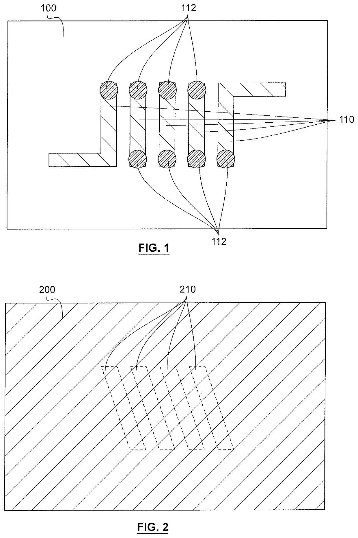
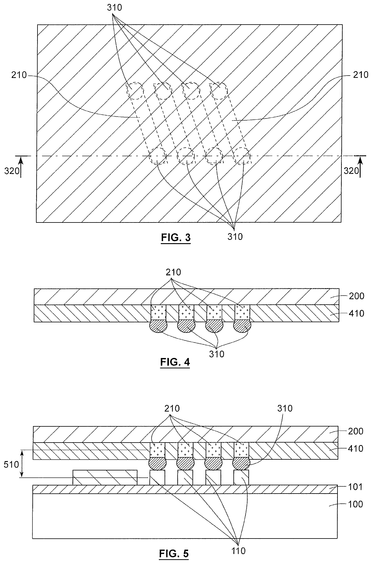
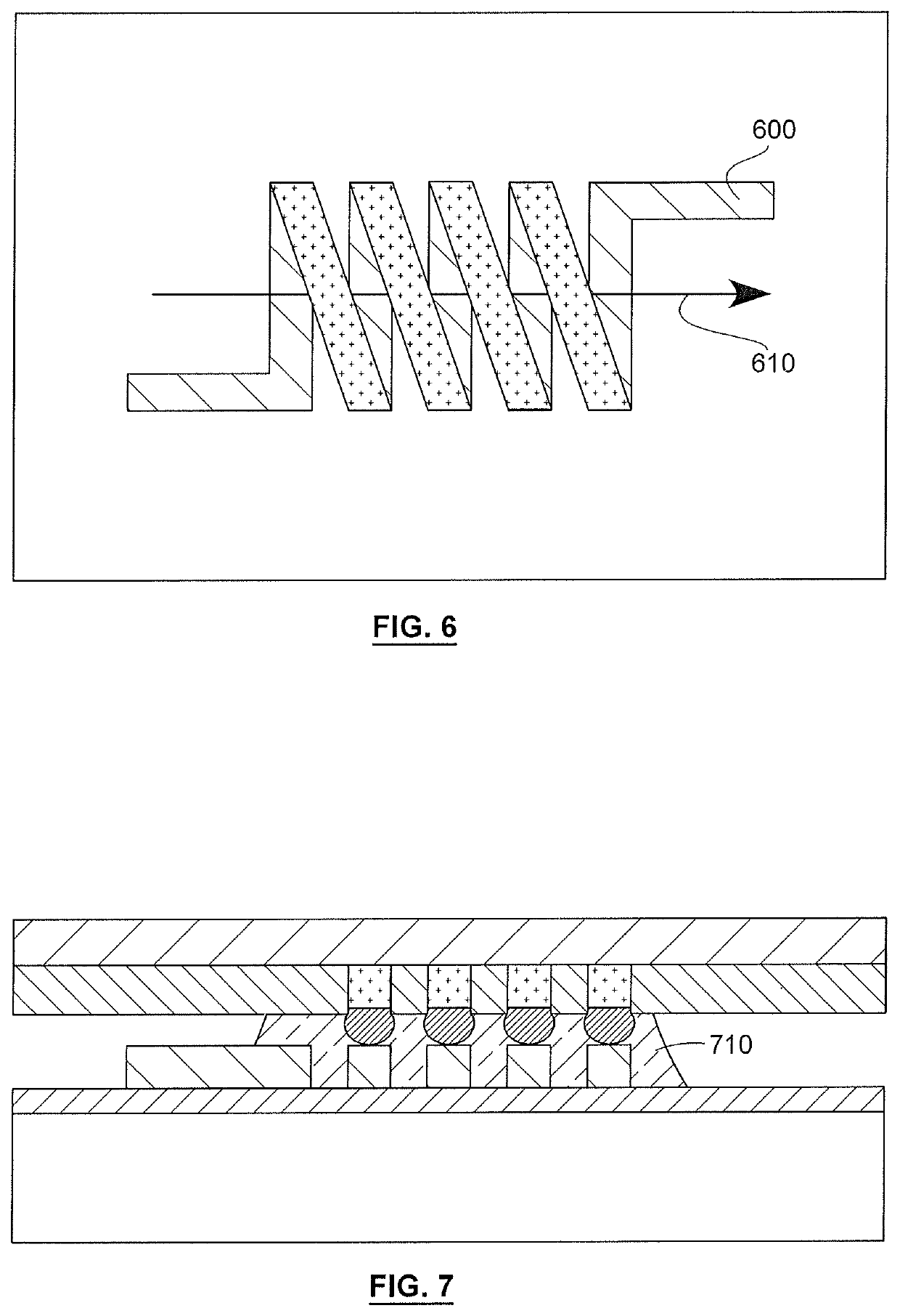
[0028]Before beginning a detailed review of the embodiments of the invention, optional characteristics are mentioned hereinafter which may be used according to any combination or alternatively:[0029]the first portion is formed on the first face of the first substrate or on a second face of the first substrate opposite the first face and / or the second portion is formed on the first face of the second substrate or on a second face of the second substrate opposite the first face;[0030]the conductive connection comprises a portion that extends into the interstitial space and comprises a portion extending into at least one of the first substrate and second substrate;[0031]the portion of the conductive connection extending into at least one of the first substrate and second substrate comprises at least one conductive via passing through said at least one of the first substrate and second substrate;[0032]it comprises at least one substrate inserted between the first substrate and the secon...


PUM

PropertyMeasurementUnit
heightsaaaaaaaaaa
thicknessaaaaaaaaaa
thicknessaaaaaaaaaa

Abstract

An inductance device includes a coil provided with at least one electrically conductive turn having a first portion of turn formed on a face of a first substrate, and a second portion of turn. A first end of the first portion is electrically connected to a first end of the second portion by a conductive connection, and the coil has a longitudinal axis, around which the at least one turn is formed, which is perpendicular to a dimension in thickness of the first substrate. The second portion is formed on a face of a second substrate different from the first substrate, with the face of the first substrate facing the face of the second substrate, with the conductive connection extending into an interstitial space located between the face of the first substrate and the face of the second substrate.

Description

FIELD OF THE INVENTION[0001]This invention in general relates to the realization of microelectronic components and more particularly of hybrid inductive components intended to be used very close with devices of the type of those produced by the microelectronics industry such as integrated circuits.TECHNOLOGICAL BACKGROUND[0002]The obtaining of microelectronic components intended to be used with the types of complex devices produced by the microelectronics industry such as integrated circuits and more generally circuits that also include mechanical and / or optical functions such as MEMS and / or NEMS (micro or nano electro mechanical systems) come up against many difficulties. This is in particular the case when it entails obtaining high electrical values from these passive components in a restricted space and as close as possible to the latter in order to limit the effects of the interference of their use in the considered application.[0003]The full integration of such a passive compon...

Claims


Application Information

Patent Timeline
Patent Type & Authority Patents(United States)
IPC IPC(8): H01F5/00H01F41/04H01F27/29H01L23/522H01L23/64H01L23/00H01F17/00H01F27/28H01L49/02H10N97/00
CPCH01L23/645H01L24/00H01F17/0013H01F27/2804H01F27/292H01L23/5227H01F41/041H01F5/00H01L2224/81815H01L2224/16H01L2224/13111H01L2924/01047H01F2017/004H01F2027/2809H01L2924/1304H01L2924/00012H01L28/10H01L2924/1306H01L2924/00014H01L2224/1411H01L24/14H01L24/13H01L2224/13014H01L24/81H01L24/16
Inventor PORNIN, JEAN-LOUISPARES, GABRIELREIG, BRUNO
Owner COMMISSARIAT A LENERGIE ATOMIQUE ET AUX ENERGIES ALTERNATIVES
Features
  • R&D
  • Intellectual Property
  • Life Sciences
  • Materials
  • Tech Scout
  • Unparalleled Data Quality
  • Higher Quality Content
  • 60% Fewer Hallucinations
Learn More