Electronic component

a technology of electronic components and shield plates, applied in the direction of resistor details, resistor housings/enclosures/embeddings, resistor mounting/supporting, etc., can solve the problems of difficult to keep spacing between adjacent conductive plates, difficult to attach shield plates, and precise management, etc., to achieve high reliability, low production costs, and high durability

Active Publication Date: 2020-04-28
MOLEX INC
View PDF17 Cites 0 Cited by
  • Summary
  • Abstract
  • Description
  • Claims
  • Application Information

AI Technical Summary

Benefits of technology

[0010]Here, an object is to provide an electronic component that is able to resolve the conventional problem described above and reliably demonstrate a desired level of performance, and that has high reliability, low production costs, and high durability, even when miniaturized.
[0016]According to this disclosure, a desired level of performance can be demonstrated, reliability is high, production costs are low, and durability is high even though an electronic component has been miniaturized.

Problems solved by technology

However, while the conductive plate 851 is held in the conventional electronic component by the housing 811, because the housing 811 is simply something given a predetermined shape through the solidification of a resin, it is difficult to keep spacing between adjacent conductive plates 851 precisely at a specified dimension, and it is difficult to attach a shield plate so as to maintain a specified gap with the conductive plate 851.
However, because it is difficult to precisely manage the dimensions of the housing 811 formed through the solidification of a resin, even when miniaturizing an electronic component having a simple structure, like the jumper chip 801, it is even more difficult to precisely maintain the gaps between the conductive plates 851 and the gaps between the shield plate and the conductive plates 851 at predetermined minute dimensions.

Method used


Image

  • Electronic component
  • Electronic component
  • Electronic component

Examples


Embodiment Construction

[0028]The embodiments will be described in detail below with reference to the drawings.

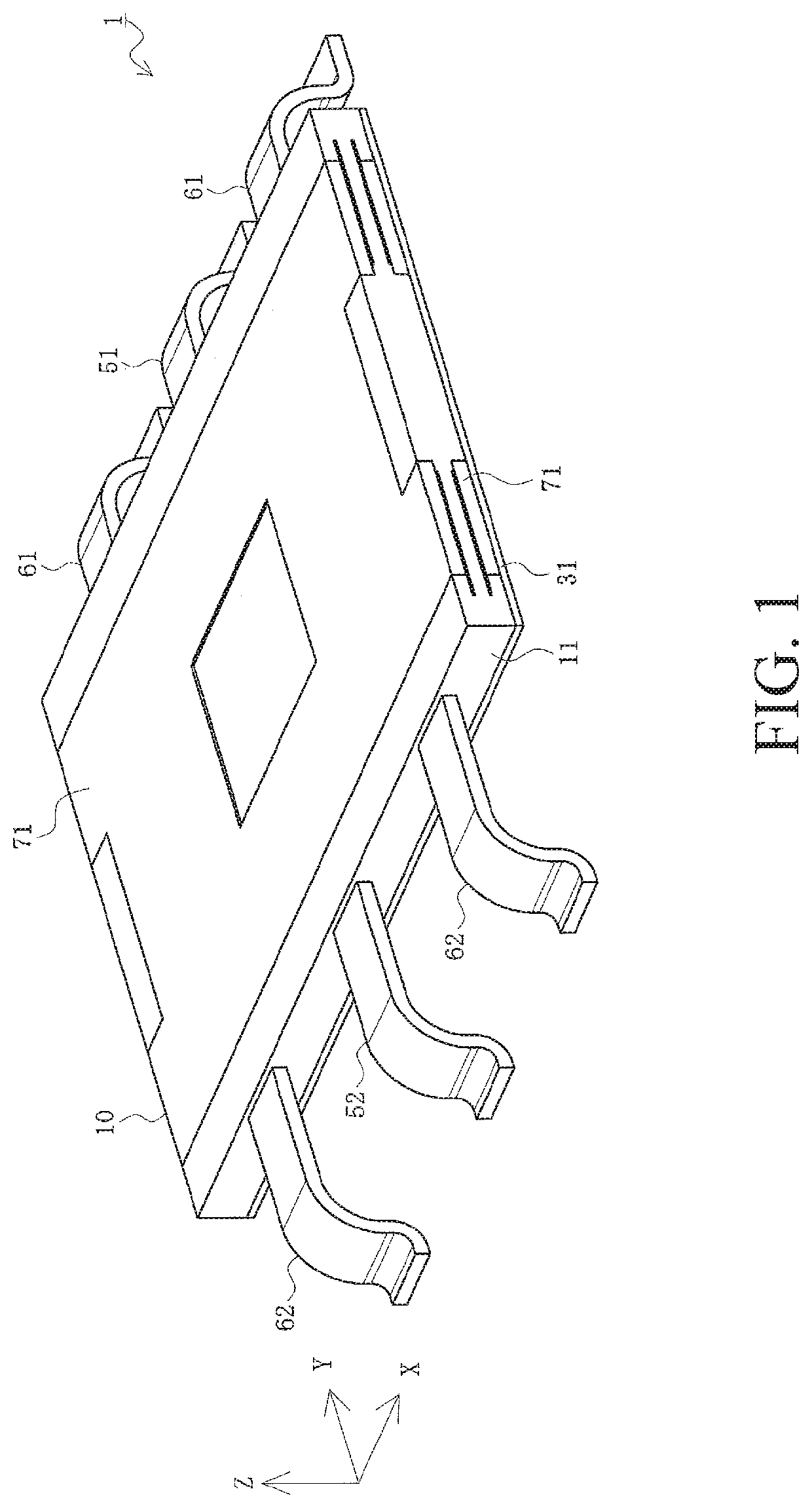
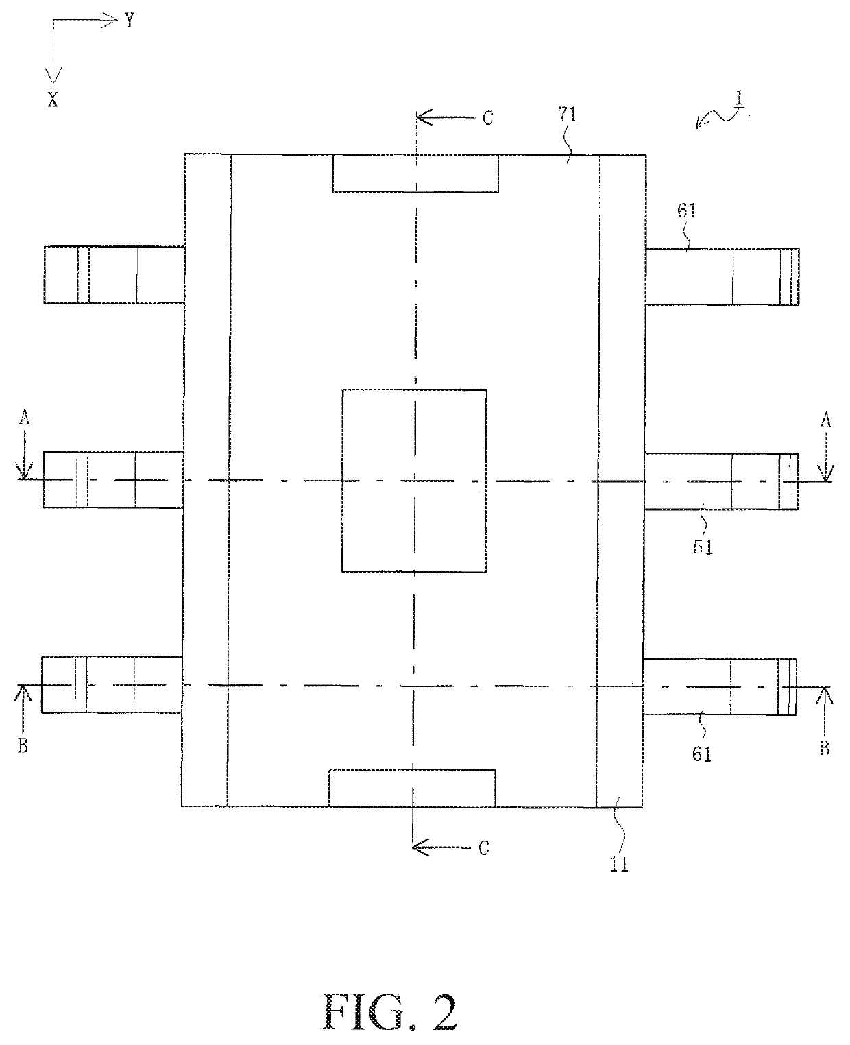
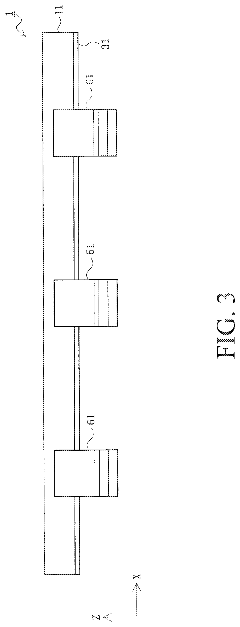
[0029]FIG. 1 is a perspective view illustrating an electronic component in the present embodiment, FIG. 2 is a top surface view of the electronic component in the present embodiment, and FIG. 3 is a side surface view of the electronic component in the present embodiment.

[0030]In the figures, 1 is an electronic component in the present embodiment and is, for example, a chip type network resistor including a resistor, that is, a resistor array, but also may be a jumper chip provided with a plurality of jumper wires, or may be something of any type. 1 is described here as a chip type electronic component—provided with a first conductor terminal (1st Terminal) 51 and a second conductor terminal (2nd Terminal) 61 that includes a resistor—that functions as a resistor array. Furthermore, while the electronic component 1 may be used in all types of equipment, such as industrial electric and electronic equ...


PUM

PropertyMeasurementUnit
thicknessaaaaaaaaaa
thicknessaaaaaaaaaa
thicknessaaaaaaaaaa

Abstract

An insulating sheet and a conductive terminal are provided in an electronic component, where at least one of the conductive terminals has a missing part, and where a remaining part positioned on both ends of the missing part is connected through a resistor element affixed to the insulating sheet.

Description

RELATED APPLICATIONS[0001]This application is a national stage of International Application No. PCT / US2017 / 036509, filed Jun. 8, 2017, which claims priority to U.S. Application No. 62 / 348,197, filed Jun. 10, 2016, and Japanese Application No. 2017-082134, filed Apr. 18, 2017, all of which are incorporated herein by reference in their entireties.TECHNICAL FIELD[0002]The present disclosure relates to an electronic component.BACKGROUND ART[0003]Conventionally, chip shaped electronic components including various elements such as resistors, and the like, are mounted on the substrates of printed circuit boards, and the like (for example, see Patent Document 1).[0004]FIGS. 11A and 11B are diagrams illustrating a conventional electronic component. Note that, FIG. 11A is a perspective view of an electronic component and FIG. 11B is a perspective view of a conductive plate.[0005]In the figure, 801 is a jumper chip, which is one type of electronic component, and is mounted on a surface of a su...

Claims


Application Information

Patent Timeline
Patent Type & Authority Patents(United States)
IPC IPC(8): H01C1/14H01C1/01H01C1/02H01C1/022
CPCH01C1/02H01C1/14H01C1/01H01C1/022H01C1/014H01C1/144H01C17/28
Inventor NIITSU, TOSHIHIRO
Owner MOLEX INC
Why Eureka
Try Eureka