System-level packaging method and packaging system based on 3D printing

a packaging method and system-level technology, applied in the field of system-level packaging methods and packaging systems based on 3d printing, can solve the problems of reducing electrical performance, complex entire manufacturing process, time-consuming and costly, etc., to reduce process and pollutant emissions complexity, improve processing efficiency, and reduce processing cost

Active Publication Date: 2020-05-05
INST OF GEOLOGY & GEOPHYSICS CHINESE ACAD OF SCI
View PDF3 Cites 0 Cited by
  • Summary
  • Abstract
  • Description
  • Claims
  • Application Information

AI Technical Summary

Benefits of technology

[0006]Based on this, it is necessary to provide a packaging method and a packaging system with high production efficiency and good packaging performance.
[0019]The chip packaging method of the present invention adopts the 3D printing method to replace the photolithography and etching steps of through via, and to replace the photolithography, etching and electroplating deposition and other process steps of the metal wires, thereby greatly reducing complexity of the process and pollutant emissions, significantly reducing the processing cost, effectively improving the processing efficiency, and being able to reduce the design and processing costs, shorten the research and development time and improve the processing accuracy and reliability. In addition, in the chip packaging method of the present invention, after the carrier and the packaging layer are removed, no redundant packaging layer is left on the back of the chip, so that the packaged chip is thinner and lighter, and the requirements of device miniaturization are satisfied.
[0021]The present system-level packaging method based on 3D printing has prominent advantages in single-piece and small-batch production. Moreover, compared with the expensive high-precision equipment in the traditional packaging manufacturing technology, the industrial-grade 3D printer is low in cost, which in turn allows large-scale production and is beneficial to the large-scale and low-cost industrial production of packaging.
[0022]Therefore, the system-level packaging method based on 3D printing of the present invention has high packaging accuracy, high production efficiency, and good product packaging performance.

Problems solved by technology

The chip must be isolated from the outside in order to prevent the chip circuit from being corroded by impurities in the air and water vapor to cause reduction of the electrical performance.
However, the traditional packaging technology has high complexity process and low precision, and requires to design and manufacture different packages for different chips, which involves the production of the mold, the complex entire manufacturing process, time-consuming and costly.
Thereby it seriously restricts the progress of research and development.

Method used


Image

  • System-level packaging method and packaging system based on 3D printing

Examples


Embodiment Construction

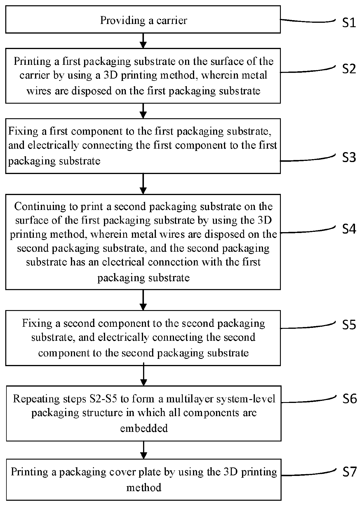
[0024]To facilitate the understanding of the present invention, the present invention will be described more fully hereinafter with reference to the drawings. The preferred embodiments of the invention are given in the drawings. However, the present invention may be implemented in many different forms and are not limited to the embodiments described herein. On the contrary, these embodiments are provided so that the contents disclosed by the present invention may be understood more thoroughly and completely.

[0025]It should be noted that when an element is referred to as being “fixed” to another element, it may be directly on the other element or there may also be an intermediate element. When an element is considered as being “connected” to another element, it can be directly connected to the other element or there may be an intermediate element at the same time.

[0026]Unless otherwise defined, all technical and scientific terms used herein have the same meanings as commonly understo...


PUM

PropertyMeasurementUnit
roughnessaaaaaaaaaa
roughnessaaaaaaaaaa
melting pointaaaaaaaaaa

Abstract

The present invention discloses a system-level packaging method and packaging system based on 3D printing. The packaging method includes the following steps: providing a carrier; printing a first packaging substrate on the surface of the carrier by using a 3D printing method, wherein metal wires are disposed on the first packaging substrate; fixing a first component to the first packaging substrate, and electrically connecting the first component to the first packaging substrate; continuing to print a second packaging substrate on the surface of the first packaging substrate by using the 3D printing method, wherein metal wires are disposed on the second packaging substrate, and the second packaging substrate has an electrical connection with the first packaging substrate; fixing a second component to the second packaging substrate, and electrically connecting the second component to the second packaging substrate; repeating the above steps to form a multilayer system-level packaging structure in which all components are embedded; and printing a packaging cover plate by using the 3D printing method. The packaging method has the advantages of simple process, low cost, less pollution, high efficiency and high reliability, and meets the requirements of system-level packaging.

Description

RELATED APPLICATIONS[0001]This application is a United States National Stage Application filed under 35 U.S.C. 371 of PCT Patent Application Serial No. PCT / CN2017 / 080784, filed Apr. 17, 2017, which claims Chinese Patent Application Serial No. CN 201610321306.6, filed May 16, 2016, the disclosure of all of which are hereby incorporated by reference in their entirety.FIELD OF THE INVENTION[0002]The present invention relates to the technical field of semiconductor packaging, and in particular to a system-level packaging method and packaging system based on 3D printing.BACKGROUND OF THE INVENTION[0003]The main function of packaging is to wrap components in a package, this not only plays a role in mounting, fixing, sealing, protecting a chip and enhancing the electrical and thermal properties, but also connects the contacts on the chip to the pins of the package through wires, and these pins are connected with other devices through wires disposed on a circuit board so as to realize the c...

Claims


Application Information

Patent Timeline
Patent Type & Authority Patents(United States)
IPC IPC(8): H01L21/48H01L21/52H01L21/683H01L23/538H01L21/67
CPCH01L21/4867H01L21/4857H01L21/52H01L21/67144H01L21/6835H01L23/5389H01L2221/68345H01L2221/68359H01L23/48H01L23/538H01L23/15H01L23/5383
Inventor LI, ZONGWEIXIONG, XINGYINHAN, KEDUYANG, CHANGCHUN
Owner INST OF GEOLOGY & GEOPHYSICS CHINESE ACAD OF SCI
Why Eureka
Try Eureka