CMOS image sensor with improved column data shift readout

a column data shift and image sensor technology, applied in the field of image sensors, can solve the problems of unwanted emi being incorporated into the image readout data stream, the array of pixels becoming much larger in the number of pixels, and the overall area being much larger, so as to improve enhance the ability to increase the readout rate of image data, and reduce power consumption and electromagnetic interference.

Active Publication Date: 2020-05-12
SMARTSENS TECH (HK) CO LTD
View PDF19 Cites 0 Cited by
  • Summary
  • Abstract
  • Description
  • Claims
  • Application Information

AI Technical Summary

Benefits of technology

[0009]An opportunity for improvement of image sensors arises when certain components are employed to enhance their ability to increase the image data readout rate while reducing power consumption and electromagnetic interference that might normally accompany an increase in readout rate. The present invention fulfills these needs and provides further advantages as described in the following summary.

Problems solved by technology

However, miniaturization has led to pixel arrays becoming much larger in the number of pixels, but not much larger in overall area due to the use of narrower interconnect lines and smaller electronic components in the pixels and in the readout and control circuits.
With the use of increased numbers of rows and columns of pixels, typical column readout circuits create larger and larger demands on power supplies resulting in the switching of larger and larger currents which result in unwanted EMI being incorporated into the image readout data stream.
The components that make up a CMOS image sensor are extremely susceptible to transients caused by the power supply.
A noisy power supply affects a pixel's ability to properly capture light, which results in a poor-quality image.
The larger and larger power supply demands also contribute to increased power consumption which trends opposite the added demand to reduce power drain on batteries in mobile devices.
A potential disadvantage of rolling shutter readout mode is spatial distortion, which results from the above.
Another disadvantage is that different regions of the exposed image will not be precisely correlated in time and appear as a distortion in the image.
However, it carries a risk of spatial distortion, especially when imaging relatively large, fast moving objects.

Method used


Image

  • CMOS image sensor with improved column data shift readout
  • CMOS image sensor with improved column data shift readout
  • CMOS image sensor with improved column data shift readout

Examples


Embodiment Construction

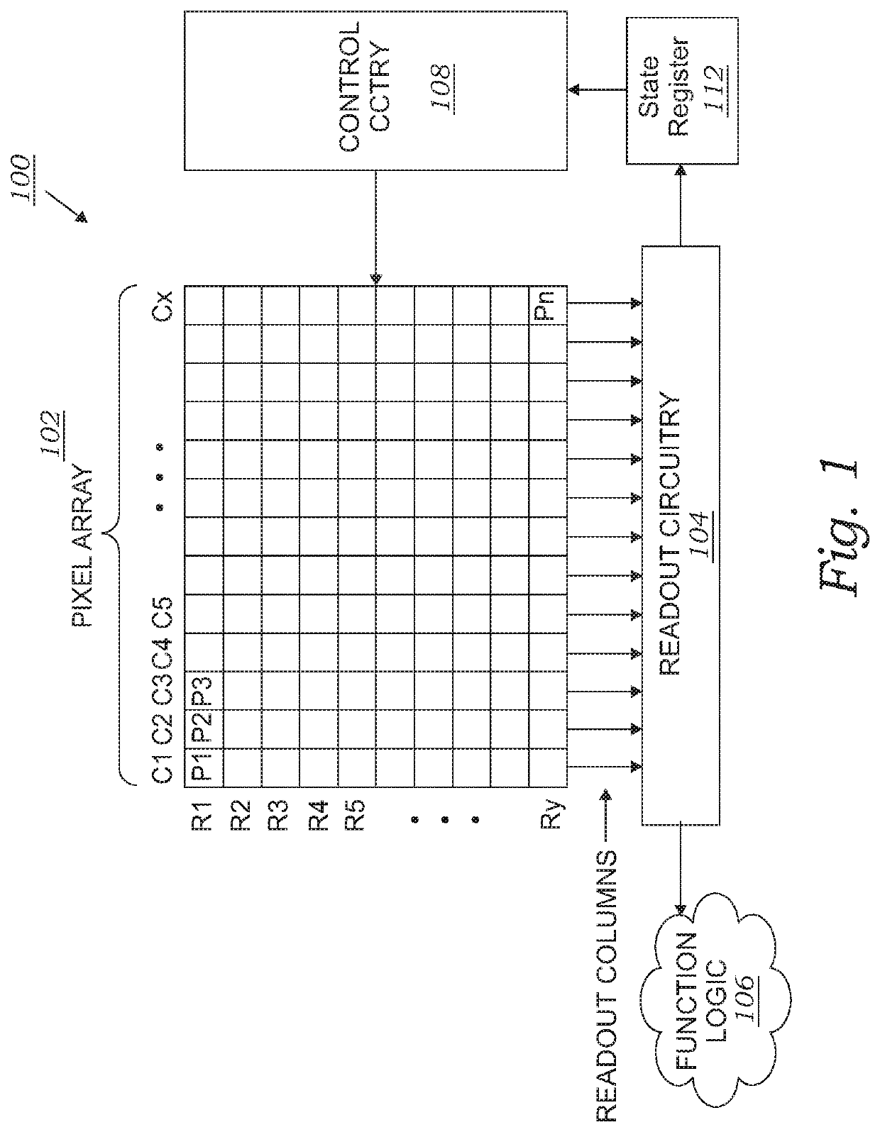
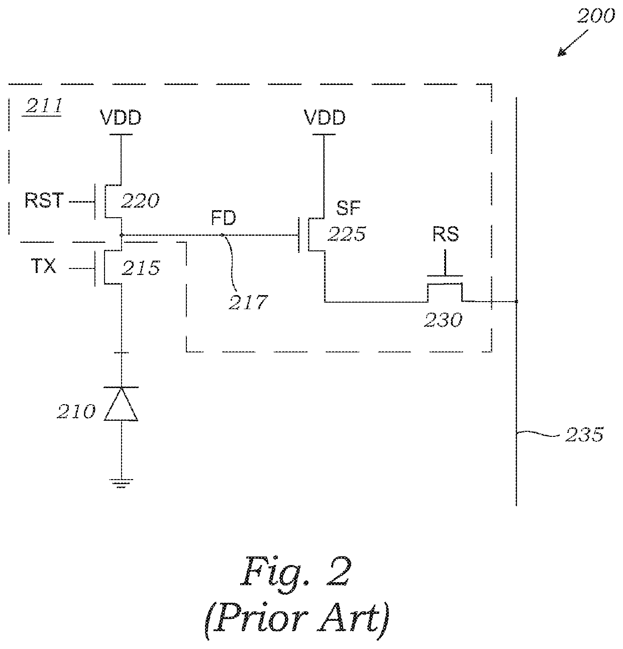
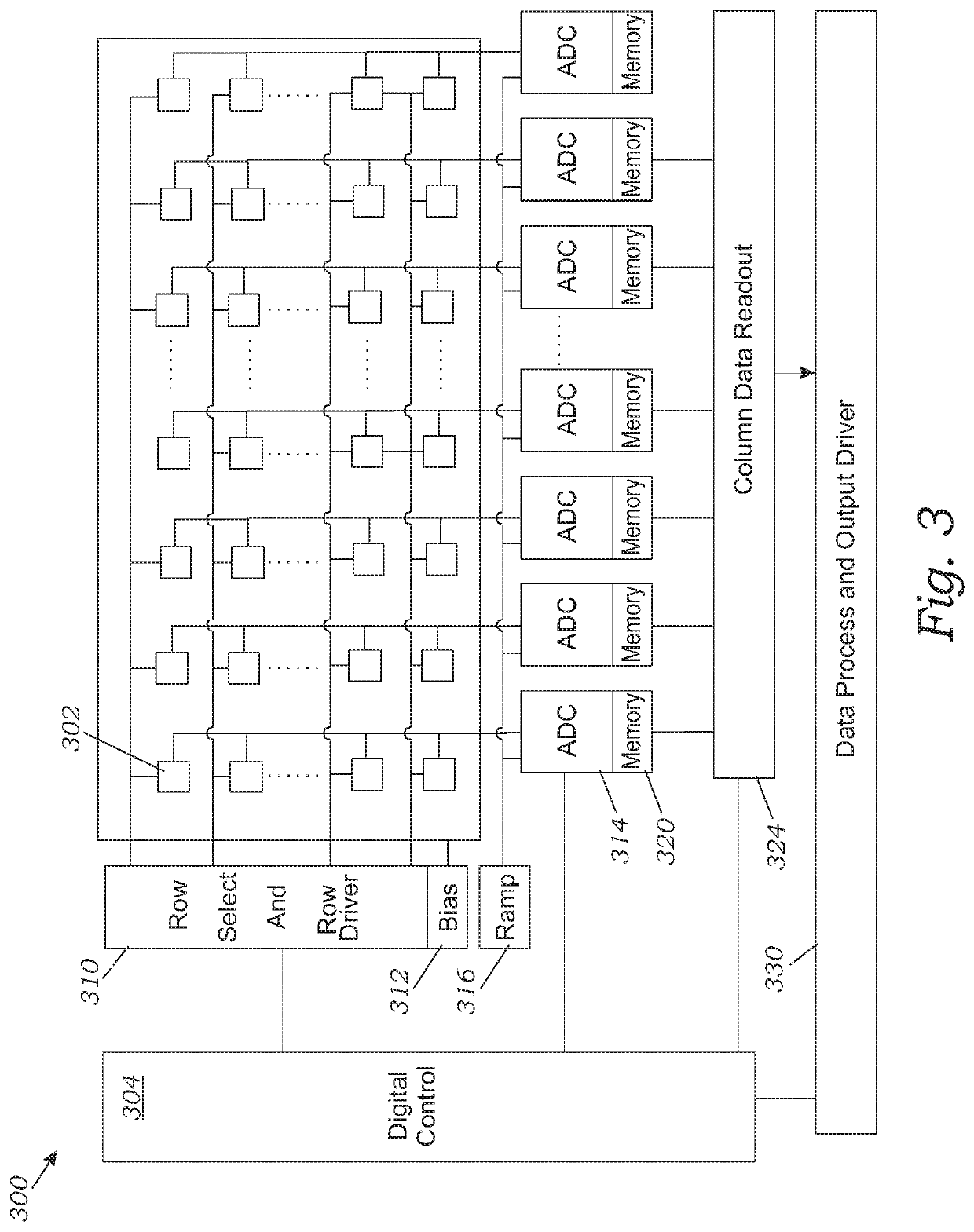
[0022]The above-described drawing figures illustrate the invention, an image sensor pixel cell array and accompanying column data readout circuits with readout rate increasing and EMI reduction circuit elements.

[0023]Various embodiments of the image sensor pixel cell are disclosed herein. In the following description, numerous specific details are set forth in order to provide a thorough understanding of the present invention. One skilled in the relevant art will recognize, however, that the techniques described herein can be practiced without one or more of the specific details, or with other methods, components, materials, etc. In other instances, well-known structures, materials, or operations are not shown or described in detail to avoid obscuring certain aspects. A substrate may have a front side and a back side. Any fabrication process that is performed from the front side may be referred to as a frontside process while any fabrication process that is performed from the back s...


PUM


Abstract

An imaging sensor having a pixel array with a separate analog-to-digital conversion (ADC) circuit coupled on an input side to each column line and on an output side to a separate M-bit wide digital memory circuit and a column data readout circuit comprising N M-bit data shifters. Each M-bit data shifter has an M-bit wide output, and single pole double throw (SPDT) switches whose common terminals provide inputs to the M-bit data shifters, wherein a first switch state of the SPDT switches connects the input of their associated M-bit data shifters to their associated M-bit wide digital memory circuits and wherein a second switch state of the SPDT switches connects the input of their associated M-bit data shifters to an M-bit wide output bus from an adjacent M-bit data shifter.

Description

BACKGROUND OF THE INVENTIONField of the Invention[0001]This invention relates generally to image sensors, and more particularly to CMOS image sensors. The present invention provides an image sensor array and circuit design to increase column memory readout rate and reduce related electromagnetic interference (EMI) when very large pixel arrays are employed. An image sensor comprising the invented circuit design may be incorporated within a digital camera.Description of Related Art[0002]An image capture device includes an image sensor and an imaging lens. The imaging lens focuses light onto the image sensor to form an image, and the image sensor converts the light into electrical signals. The electric signals are output from the image capture device to other components of a host electronic system. The image capture device and the other components of a host electronic system form an imaging system. Image sensors have become ubiquitous and may be found in a variety of electronic systems...

Claims


Application Information

Patent Timeline
Patent Type & Authority Patents(United States)
IPC IPC(8): H04N5/374H04N5/372H04N5/347H04N5/3745H04N9/04H04N5/335H04N5/378
CPCH04N5/335H04N5/3742H04N5/37455H04N5/347H04N9/045H04N5/37213H04N5/37457H04N5/378H04N25/767H04N25/75H04N23/10H04N25/00H04N25/46H04N25/713H04N25/772H04N25/778
Inventor XU, CHENMO, YAOWUHOU, JINJIANMA, WEIJIANREN, GUANJING
Owner SMARTSENS TECH (HK) CO LTD
Why Eureka
Try Eureka