Wired circuit board including a conductive pattern having a wire and a dummy portion

a wired circuit board and conductive pattern technology, applied in the direction of conductive pattern formation, conductive material removal by irradiation, head carrier alignment, etc., can solve the problem of inadequate formation of wiring patterns that cannot be prevented, and achieve excellent connection reliability, high degree of freedom, and improved wire reliability

Active Publication Date: 2020-06-16
NITTO DENKO CORP
View PDF53 Cites 0 Cited by
  • Summary
  • Abstract
  • Description
  • Claims
  • Application Information

AI Technical Summary

Benefits of technology

[0019]Therefore, a conductive pattern having high reliability can be provided with a high degree of freedom.
[0060]In the wired circuit board of the present invention, the reliability of the wire is improved.

Problems solved by technology

Then, there are disadvantages in that inadequate formation of the wiring pattern cannot be prevented.

Method used


Image

  • Wired circuit board including a conductive pattern having a wire and a dummy portion
  • Wired circuit board including a conductive pattern having a wire and a dummy portion
  • Wired circuit board including a conductive pattern having a wire and a dummy portion

Examples


first embodiment

4. Modified Example of First Embodiment

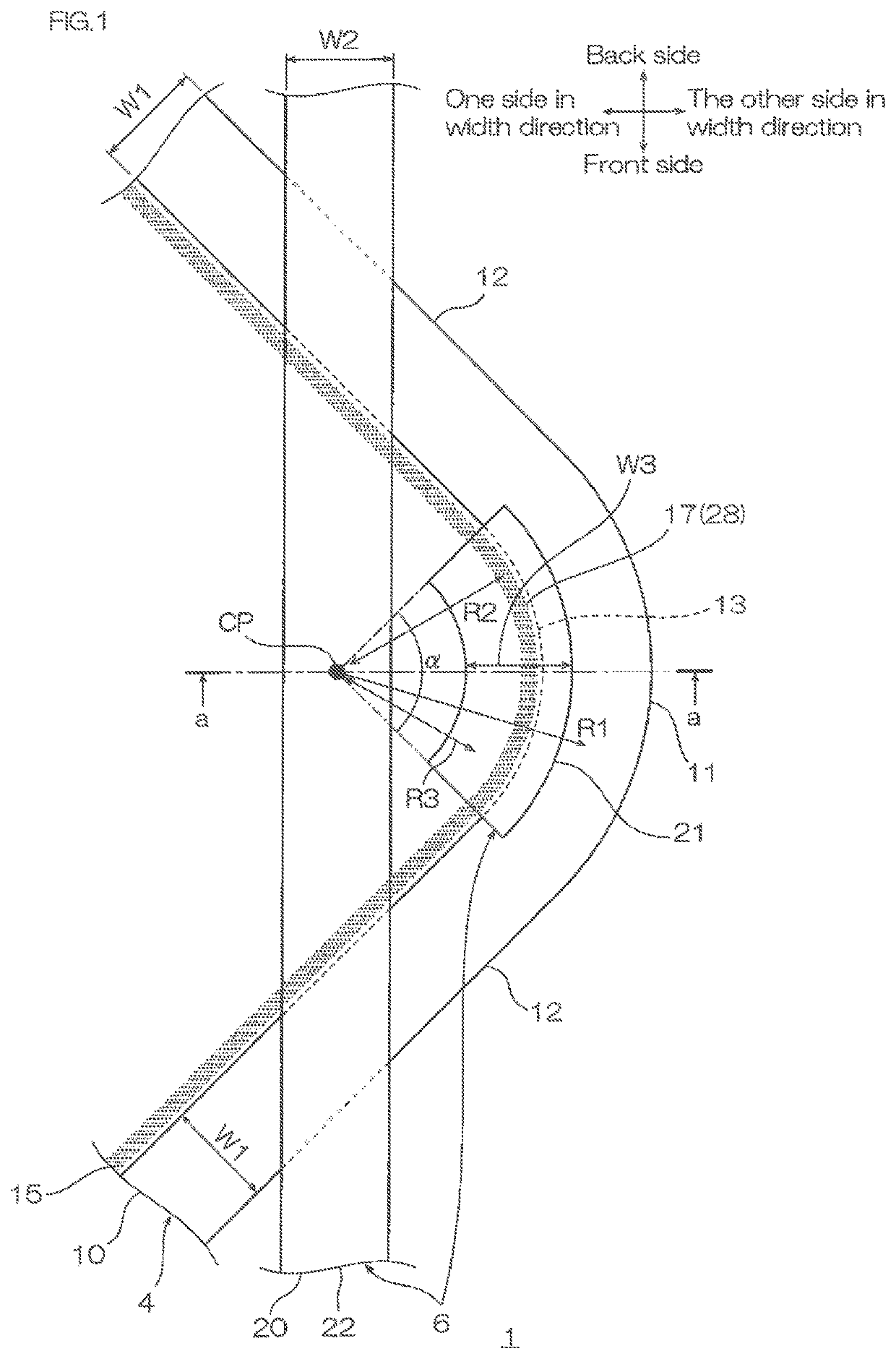
[0234]In the first embodiment, the bent portion 17 as an example of the bent portion is used. Alternatively, for example, the bent portion is not limited to the bent portion 17.

[0235]Although not shown, a curved portion that is curved at a predetermined angle in one direction in a plurality of times or a single time (or a curving portion that curves at a predetermined angle in one direction) can be also used. In such a case, the curved portion (curving portion) includes a part of vertexes and at least two sides continued therefrom of a polygon. The above-described angle, is for example, more than 0 degree, preferably 30 degrees or more, and for example, 90 degrees or less, preferably 60 degrees or less.

[0236]As shown in FIG. 1, the shape of the dummy wire 21 is a generally are shape when viewed from the top, and the shape thereof is not limited to the above-described shape as long as the dummy wire 21 is overlapped with the second portion 28 in...

second embodiment

[0238]In the second embodiment, for the members and steps that are the same as the first embodiment, the same reference numerals are given and detailed descriptions thereof are omitted.

[0239]In the first embodiment, the negative type photoresist 25 is used, and the additive method is used to form the second conductive pattern 6.

[0240]However, in the second embodiment, the positive type photoresist 25 is used, and the subtractive method is used to form the second conductive pattern 6.

[0241]4-1. Method for Producing a Wired Circuit Board

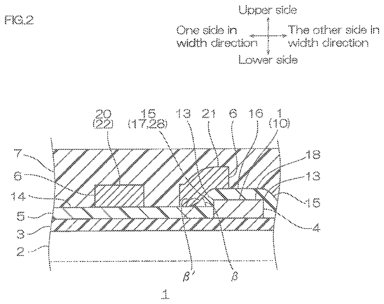
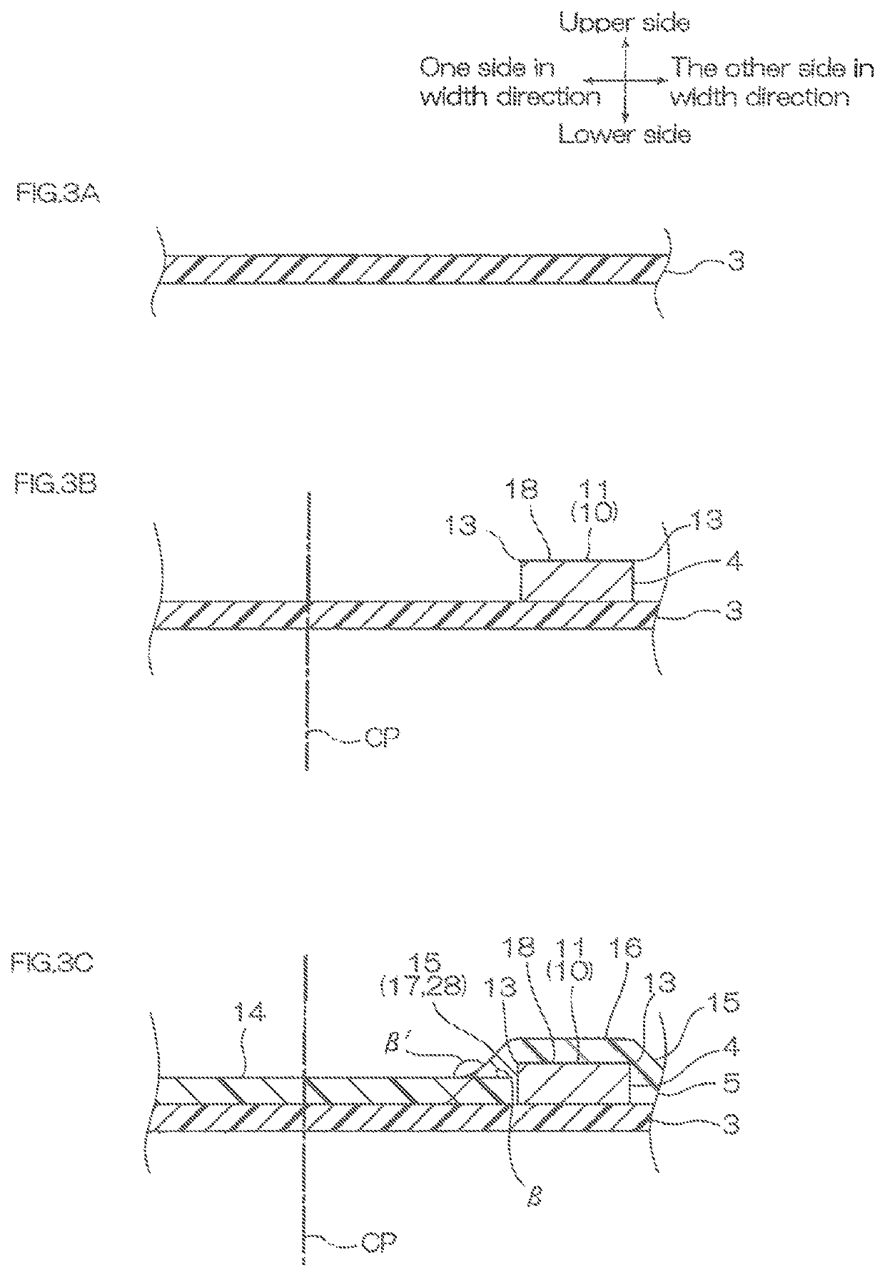
[0242]The production method of the wired circuit board 1 of the second embodiment includes a step (i) (ref: FIG. 3A), in which the insulating base layer 3 of the first embodiment is prepared, a step (ii) (ref: FIG. 3B), in which the first conductive pattern 4 is provided, and a step (1) (ref: FIG. 3C), in which the intermediate insulating layer 5 is provided.

[0243]The production method of the wired circuit board 1 of the second embodiment further inclu...

third embodiment

3. Modified Example of Third Embodiment

[0291]The wired circuit board 1 of the third embodiment is produced using the negative type photoresist 25. In the modified example, though not shown, the wired circuit board 1 of the third embodiment can be also produced using the positive type photoresist 25.

[0292]As shown in FIG. 11, the shape of the dummy portion 35 is a generally triangular shape when viewed from the top, and the shape thereof is not limited to the above-described shape as long as the dummy portion 35 is overlapped with the second portion 28 in the thickness direction.

[0293]The dummy portion 35 is overlapped with only the second portion 28 corresponding to the first arc portion 11, and furthermore, can be also overlapped with the second portion 28 corresponding to the first linear portion 12.

Fourth Embodiment

[0294]In the fourth embodiment, for the members and steps that are the same as the first to third embodiments, the same reference numerals are given and detailed descr...


PUM

PropertyMeasurementUnit
widthaaaaaaaaaa
angleaaaaaaaaaa
angleaaaaaaaaaa

Abstract

A method for producing a wired circuit board including an insulating layer and a conductive pattern, including (1), providing the insulating layer having an inclination face; (2), providing a metal thin film at least on the surface of the insulating layer; (3), providing a photoresist on the surface of the metal thin film; (4), disposing a photomask so that a first portion, where the conductive pattern is provided in the photoresist, is shielded from light, and the photoresist is exposed to light through the photomask; (5), removing the first portion to expose the metal thin film corresponding to the first portion; and (6), providing the conductive pattern on the surface of the metal thin film exposed from the photoresist. The inclination face has a second portion that allows the light reflected at the metal thin film to reach the first portion.

Description

[0001]The present application claims priority from Japanese Patent Application No. 2016-077551 filed on Apr. 7, 2016, the contents of which are hereby incorporated by reference into this application.BACKGROUND OF THE INVENTIONField of the Invention[0002]The present invention relates to a wired circuit board and a production method thereof, in particular, to a method for producing a wired circuit board, and a wired circuit board produced by the method.Description of Related Art[0003]It has been known that a wired circuit board is produced by providing an insulating layer and a wiring pattern thereon.[0004]For example, Japanese Unexamined Patent Publication No. 2014-127216 has proposed a method for producing a suspension board with circuit: the method includes a step of forming a first portion having a first thickness and a second portion having a second thickness that is smaller than the first thickness in the insulating layer, and a step of forming a wiring pattern so as to extend o...

Claims


Application Information

Patent Timeline
Patent Type & Authority Patents(United States)
IPC IPC(8): H05K3/02G11B5/60H05K1/02H05K3/46H05K3/10
CPCG11B5/60H05K3/027H05K1/0296H05K3/4685H05K2201/09727H05K2201/09781H05K3/108H05K2203/0562H05K2201/09272H05K2201/09018H05K1/0278H05K1/056H05K2201/0191
Inventor SUGIMOTO, YUUTANABE, HIROYUKIFUJIMURA, YOSHITO
Owner NITTO DENKO CORP
Why Eureka
Try Eureka