

Memory structure
a memory structure and memory technology, applied in the field of memory structure, can solve problems such as the difficulty of accurately connecting the contact to the select gate of the spacer form
- Summary
- Abstract
- Description
- Claims
- Application Information
AI Technical Summary
Benefits of technology
Problems solved by technology
Method used
Image

Examples
Embodiment Construction
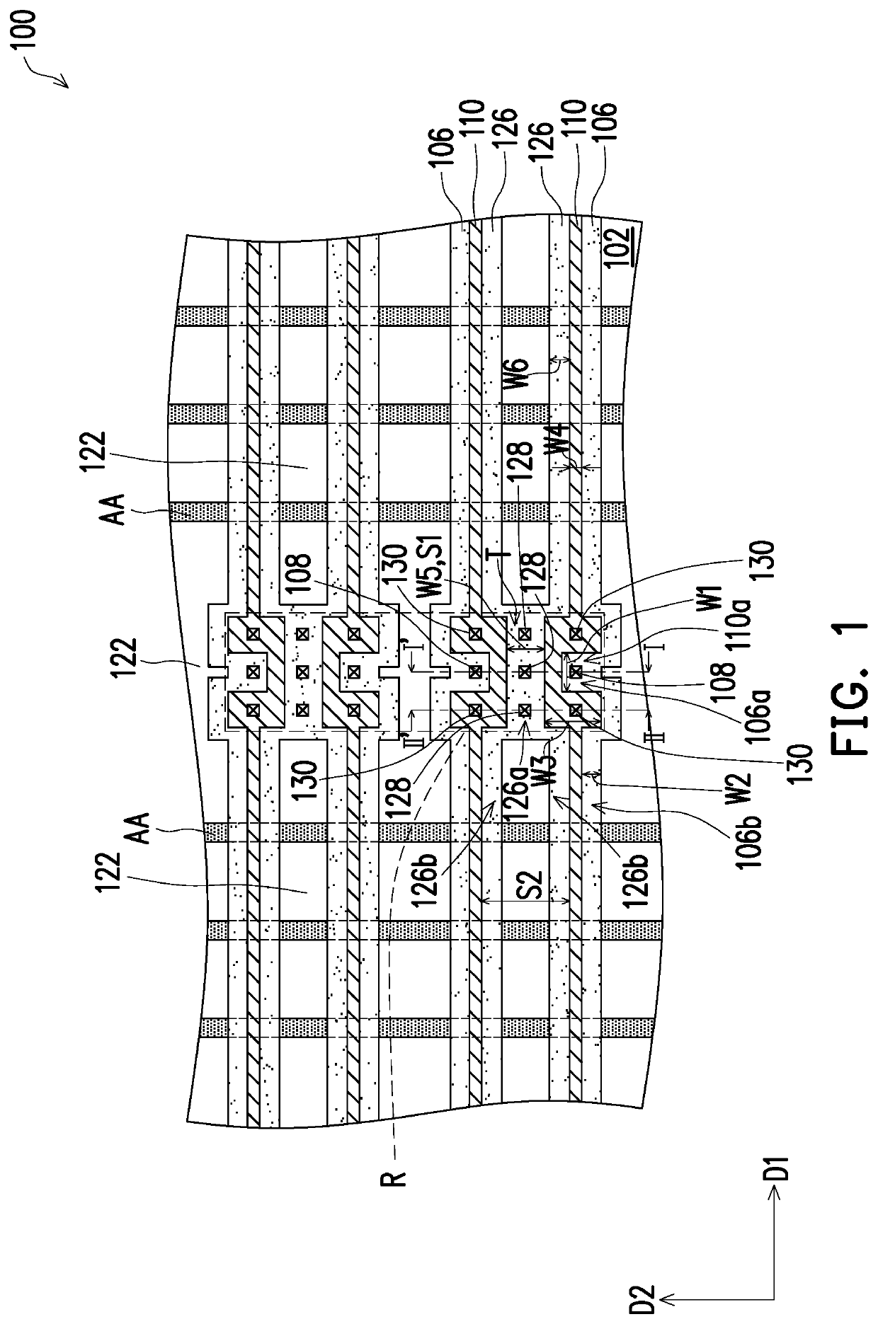
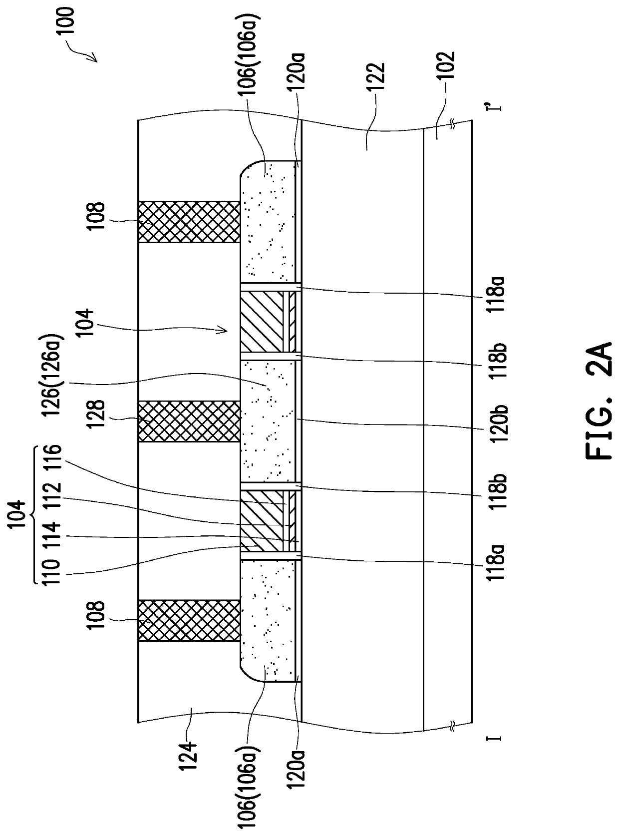
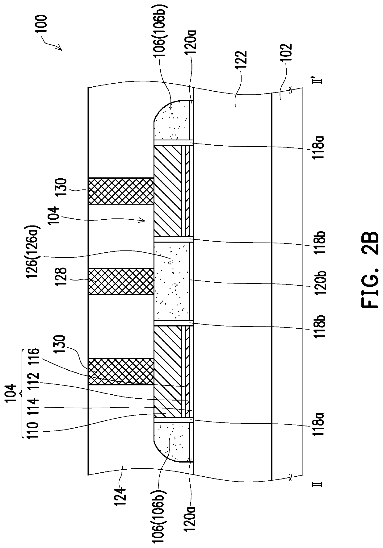
[0033]FIG. 1 is a top view of a memory structure according to an embodiment of the invention. FIG. 2A is a cross-sectional view taken along a sectional line I-P depicted in FIG. 1. FIG. 2B is a cross-sectional view taken along a sectional line II-IP depicted in FIG. 1. In the top view of FIG. 1, some of the components in FIG. 2A and FIG. 2B are omitted to clearly illustrate the relationship between the components of FIG. 1.
[0034]Referring to FIG. 1, FIG. 2A, and FIG. 2B, a memory structure 100 includes a substrate 102, at least one stacked gate structure 104, a spacer conductive layer 106, and a contact 108. The memory structure 100 is, for example, a non-volatile memory structure, but the invention is not limited thereto. The substrate 102 is, for example, a semiconductor substrate such as a silicon substrate.
[0035]The stacked gate structure 104 is disposed on the substrate 102 and includes a control gate 110. When the number of stacked gate structures 104 is multiple, each of the ...
PUM
| Property | Measurement | Unit |
|---|---|---|
| width | aaaaa | aaaaa |
| conductive | aaaaa | aaaaa |
| charge storage | aaaaa | aaaaa |
Abstract
Description
Claims
Application Information