
Plasma display panel

a display panel and plasma technology, applied in the direction of discharge tube luminescnet screens, address electrodes, gas-filled discharge tubes, etc., can solve the problems of increasing the distance between the address electrodes, increasing the amount of energy or power (cvsup>2/sup>f), and increasing the power consumption of the address electrodes. direct connection, reducing crosstalk, and improving discharge efficiency

Inactive Publication Date: 2007-03-15
SAMSUNG SDI CO LTD
View PDF1 Cites 0 Cited by
  • Summary
  • Abstract
  • Description
  • Claims
  • Application Information

AI Technical Summary

Benefits of technology

[0011] An aspect of the present invention provides a plasma display panel having two address electrodes assigned to each pixel to reduce power consumption without degrading resolution, the address electrodes having a large line width to improve address discharge efficiency.
[0016] As a smaller number of address electrodes are used while maintaining the same resolution, the distance between the address electrodes increases. This substantially reduces crosstalk among the address electrodes, as well as heat generation.
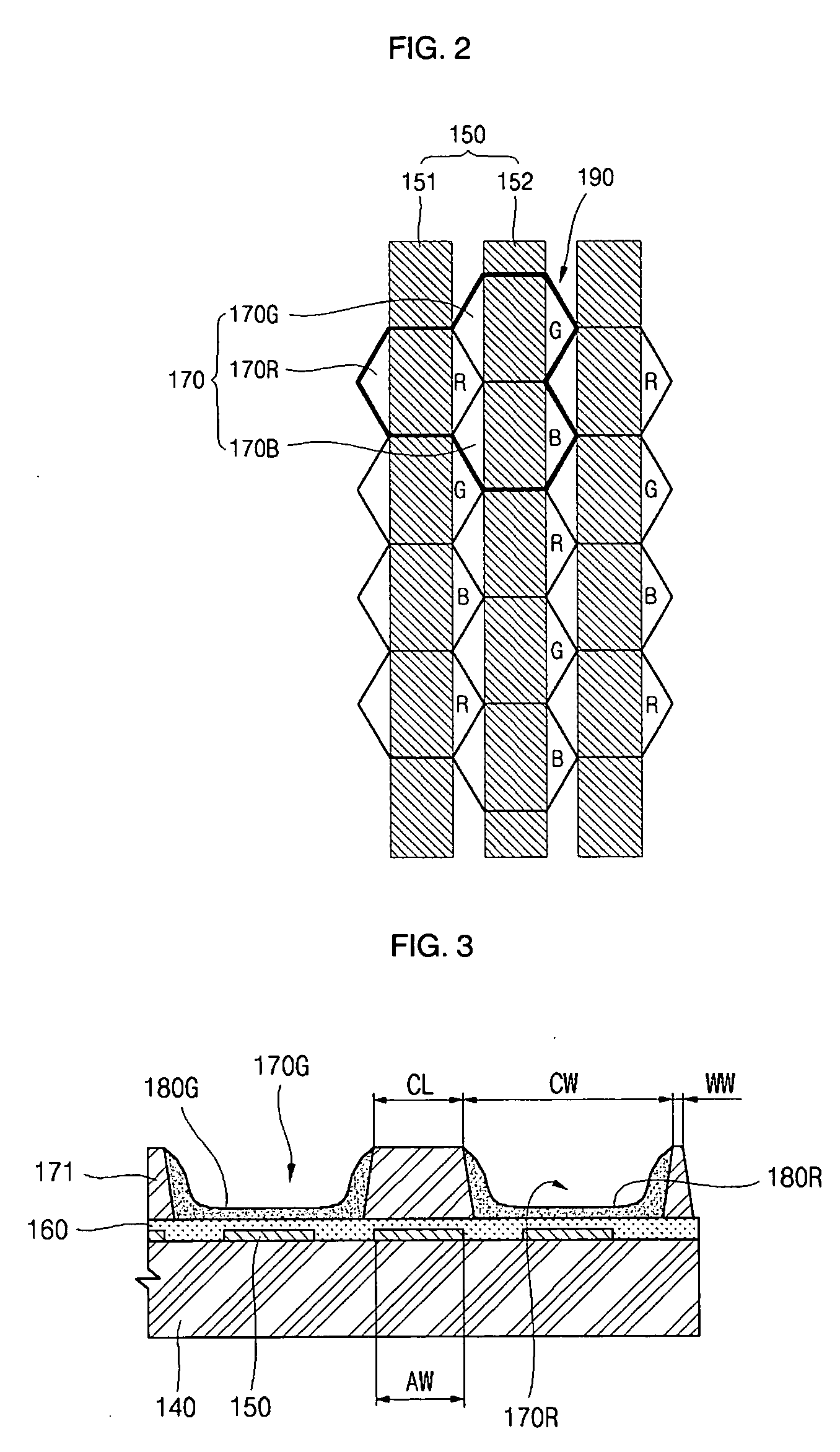
[0017] The line width of the address electrodes of the plasma display panel according to an embodiment of the present invention is substantially larger than that of the prior art (for example, the line width of the address electrodes ranges from 80 to 120% of a length of a side of the barriers, ranges from 40 to 60% of a maximum width of the discharge cells, and / or ranges from 90 to 150 μm) to improve the discharge efficiency during addressing discharge. This is because increase in the line width of the address electrodes increases the discharge area. Such improvement of the address discharge efficiency assists (or ensures or guarantees) addressing of selected discharge cells, as well as following display discharge. In addition, such improvement of the address discharge efficiency reduces power consumption and the burden on circuits for driving the address electrodes, because the address voltage does not need to be increased very much.
[0018] The addressing time is shortened by such improvement of the addressing discharge efficiency. Consequently, the display discharge time can be increased by as much as the addressing time is shortened. This improves the luminance, contrast, and optical efficiency of the plasma display panel.

Problems solved by technology

However, when the pitch between the address electrodes decreases, the capacitance between the address electrodes increases, and the amount of energy or power (CV2f) consumed between the address electrodes is also increased.
In addition, increase in power consumption of the address electrodes is directly connected to increase in overall power consumption of the plasma display panel, because the discharge voltage applied to the address electrodes is larger than the voltage applied to the display electrodes.
Also, as the distance between the address electrodes decreases, severe crosstalk may occur.
This degrades the address discharge efficiency.
Such degradation may result in addressing failure and cause specific discharge cells to malfunction.
However, the larger the address voltage is, the more severe crosstalk becomes.
This may generate erroneous discharge.
This increases power consumption.
However, the longer the addressing time is, the shorter the display discharge time becomes.
This degrades the luminance, contrast, and optical efficiency of the plasma display panel.

Method used


Image

  • Plasma display panel
  • Plasma display panel
  • Plasma display panel

Examples


Embodiment Construction

[0024] In the following detailed description, only certain exemplary embodiments of the present invention are shown and described, by way of illustration. As those skilled in the art would recognize, the described exemplary embodiments may be modified in various ways, all without departing from the spirit or scope of the present invention. Accordingly, the drawings and description are to be regarded as illustrative in nature, and not restrictive.

[0025] There may be parts shown in the drawings, or parts not shown in the drawings, that are not discussed in the specification as they are not essential to a complete understanding of the invention. Like reference numerals designate like elements.

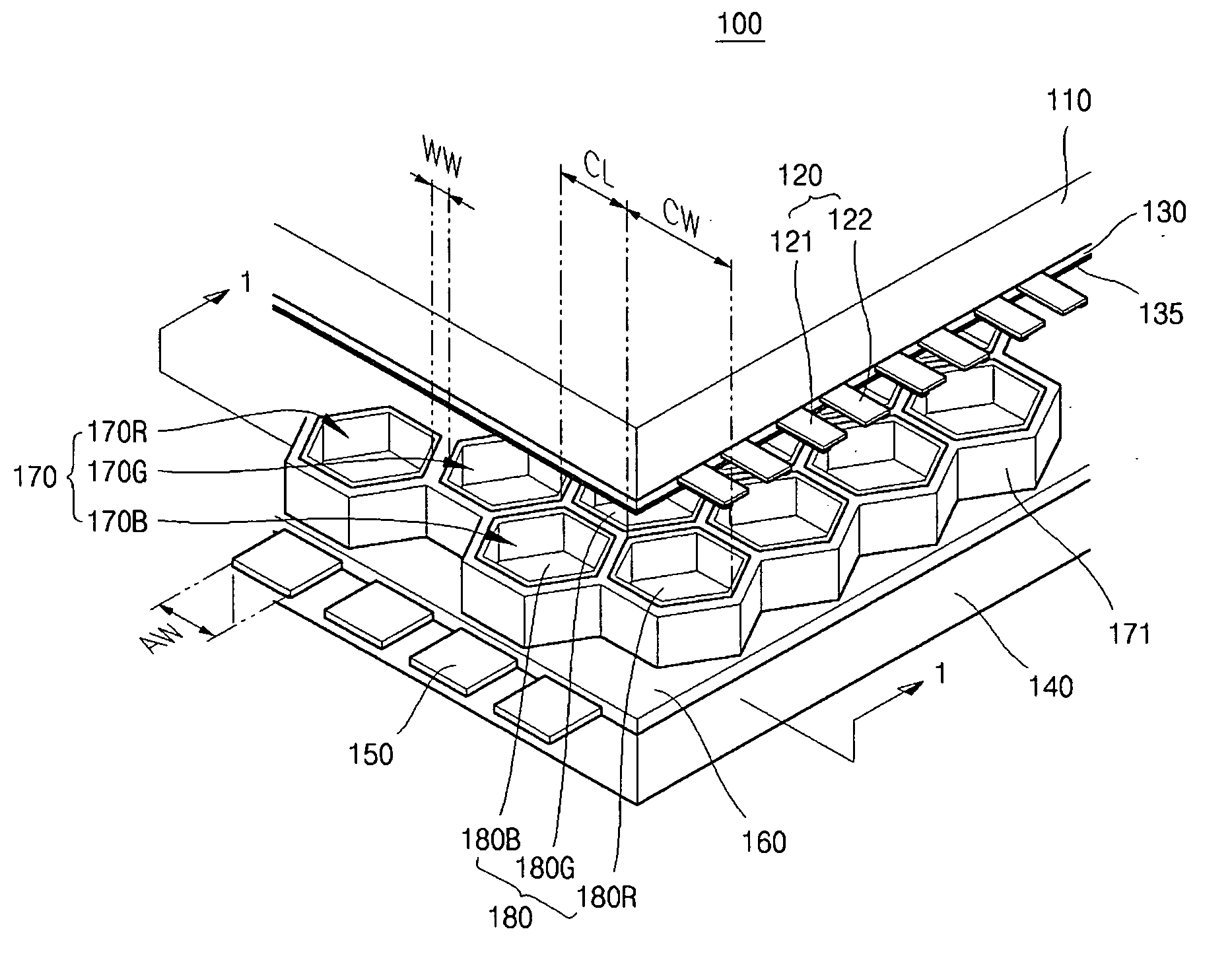
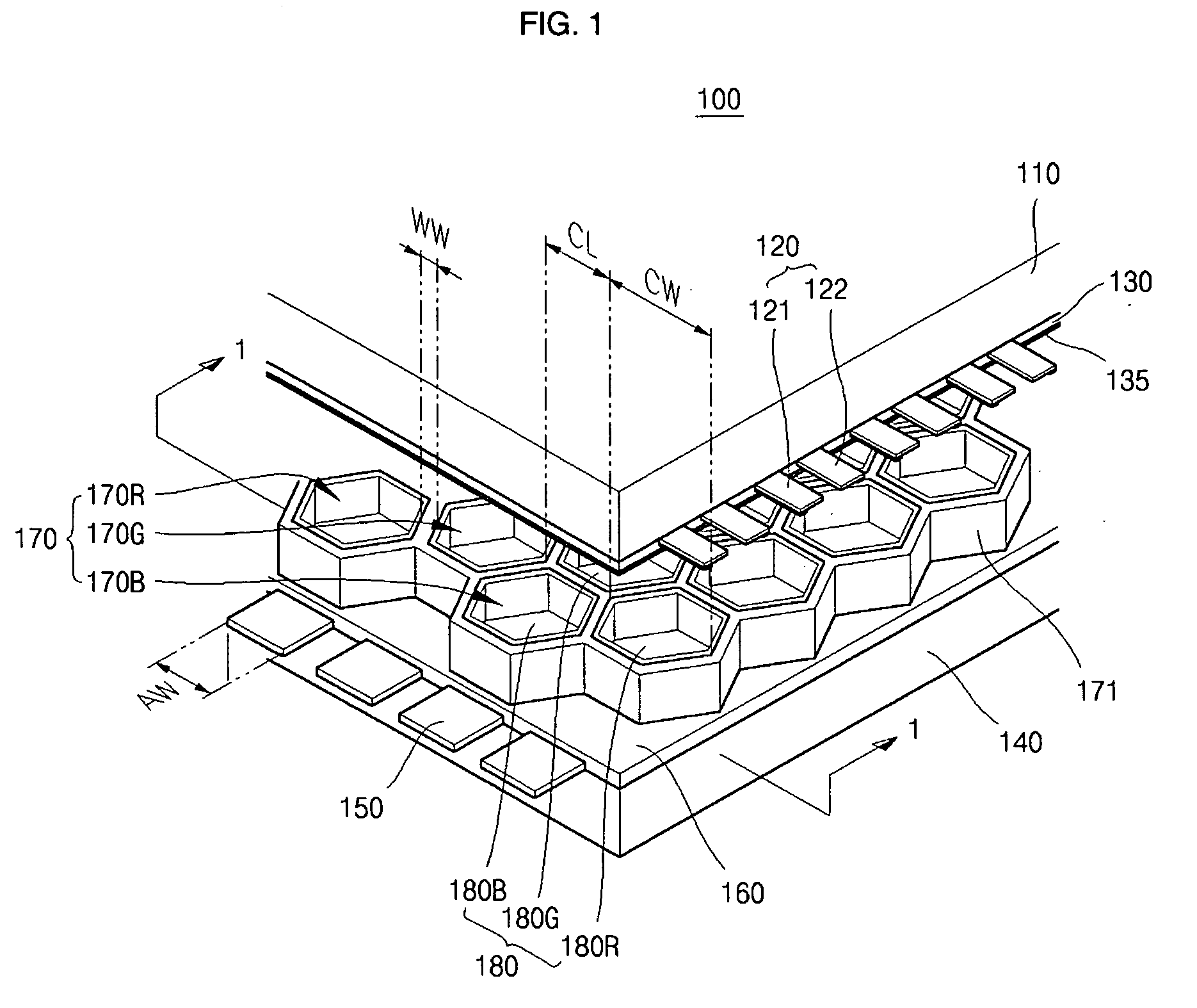
[0026]FIG. 1 is a partially broken perspective view showing a plasma display panel according to an embodiment of the present invention.

[0027] As shown in FIG. 1, the plasma display panel 100 includes a front glass substrate 110; a number of display electrodes 120 formed on the front glass subst...


PUM


Abstract

A plasma display panel having two address electrodes assigned to each pixel to reduce power consumption without degrading resolution, the address electrodes having a large line width to improve address discharge efficiency. In one embodiment, three neighboring discharge cells for emitting different colors of visible rays define a pixel, two address electrodes are assigned to each pixel, and the address electrodes have a line width not less than a length of a side of a plurality of barriers defining the discharge cells. In the embodiment, the line width of the address electrodes may range from about 90 to about 150 μm.

Description

CROSS-REFERENCE TO RELATED APPLICATION [0001] The present application claims priority to and the benefit of Korean Patent Application No. 10-2005-0080064, filed on Aug. 30, 2005, in the Korean Intellectual Property Office, the entire content of which is incorporated herein by reference. BACKGROUND OF THE INVENTION [0002] 1. Field of the Invention [0003] The present invention relates to a plasma display panel, and more particularly, to a plasma display panel having two address electrodes assigned to each pixel to reduce power consumption without degrading resolution, the address electrodes having a large line width to improve address discharge efficiency. [0004] 2. Description of the Related Art [0005] A plasma display panel includes a front glass substrate incorporated with a number of display electrodes and a rear glass substrate incorporated with a number of address electrodes. The address electrodes cross (or intersect with) the display electrodes. A number of barriers are formed...

Claims


Application Information

Patent Timeline
IPC IPC(8): H01J1/62H01J11/12H01J11/32
CPCH01J11/12H01J2211/365H01J2211/265H01J11/32H01J11/26H01J11/36
Inventor KIM, TAEWOOYIM, SANGHOON
Owner SAMSUNG SDI CO LTD
Learn More