Semiconductor device
a technology of semiconductors and circuits, applied in the direction of semiconductor devices, electrical devices, transistors, etc., can solve the problems of high degree of technical difficulty in preventing the breakage of the silicided portion, delay in circuit operation, etc., to prevent an increase in circuit delay and prevent a circuit malfunction
- Summary
- Abstract
- Description
- Claims
- Application Information
AI Technical Summary
Benefits of technology
Problems solved by technology
Method used
Image
Examples
first embodiment
(First Embodiment)
[0033]Referring to the drawings, an explanation is given of a first embodiment according to the present invention.
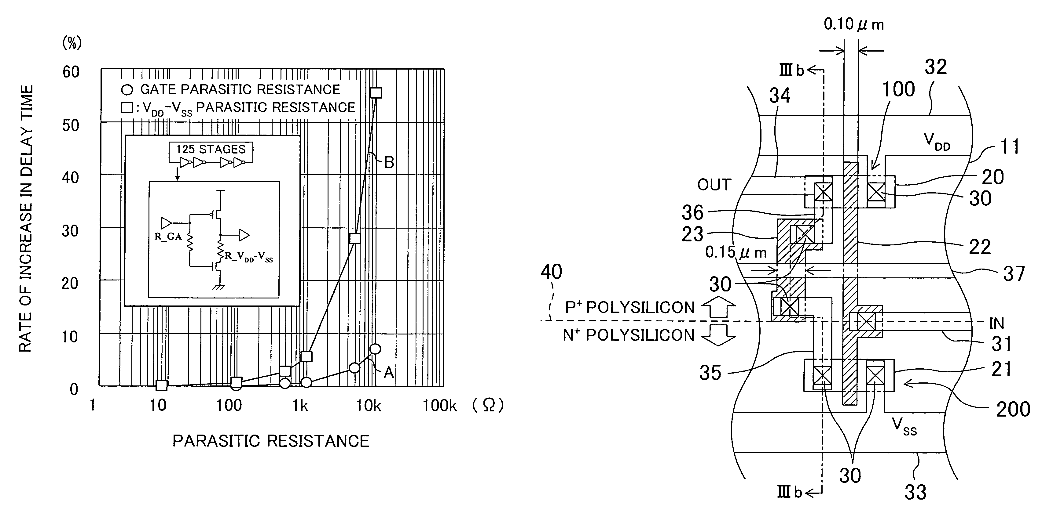
[0034]FIG. 3A is a plan view illustrating a semiconductor device according to a first embodiment of the present invention and FIG. 3B is a sectional view cut along the line IIIb—IIIb shown in FIG. 3A.
[0035]As shown in FIG. 3A and FIG. 3B, a p-type diffusion region 20 and an n-type diffusion region 21 are formed at the top of a semiconductor substrate 10 made of silicon (Si), for example. The p-and n-type diffusion regions 20 and 21 are divided by isolation regions 11 to be spaced from each other.
[0036]On the isolation regions 11 surrounding the p-type diffusion region 20 and the n-type diffusion region 21, a line-shaped gate electrode 22 made of polysilicon having a silicided top portion is formed. Thus, a p-type MOS transistor 100 is made up of the p-type diffusion region 20 and the gate electrode 22 and an n-type MOS transistor 200 is made up of the n...
second embodiment
(Second Embodiment)
[0051]Hereinafter, an explanation is given of a second embodiment of the present invention with reference to the drawings.
[0052]FIG. 4 shows a planar configuration of a semiconductor device according to the second embodiment of the present invention. In FIG. 4, the same components as those shown in FIG. 3A are given with the same reference numerals and explanations thereof are omitted.
[0053]An explanation is given only of the differences from the semiconductor device of the first embodiment. As shown in FIG. 4, a second shared line 23A is formed not only in a region nearer the p-type MOS transistor 100 in relation to the boundary 40 but also in a region nearer the n-type MOS transistor 200 in relation to the boundary 40, i.e., the second shared line 23A is formed to cross the boundary 40. Therefore, in the second shared line 23A, part of a lower portion thereof nearer the p-type MOS transistor 100 in relation to the boundary 40 is made of p-type polysilicon and th...
PUM
 Abstract
Description
Claims
Application Information


