Organic electroluminescent device and method for producing same

a technology of electroluminescent devices and organic el, which is applied in the direction of electroluminescent light sources, identification means, instruments, etc., can solve problems such as uneven display, and achieve the effect of improving moisture resistance reliability

Active Publication Date: 2020-06-23
SAKAI DISPLAY PROD
View PDF39 Cites 2 Cited by
  • Summary
  • Abstract
  • Description
  • Claims
  • Application Information

AI Technical Summary

Benefits of technology

[0028]An embodiment of the present invention provides an organic EL device, including a thin film encapsulation structure, that has an improved moisture-resistance reliability, and a method for producing the same.

Problems solved by technology

An OLED (especially, an organic light emitting layer and a cathode electrode material) is easily influenced by moisture to be deteriorated and to cause display unevenness.

Method used


Image

  • Organic electroluminescent device and method for producing same
  • Organic electroluminescent device and method for producing same
  • Organic electroluminescent device and method for producing same

Examples


embodiment 1

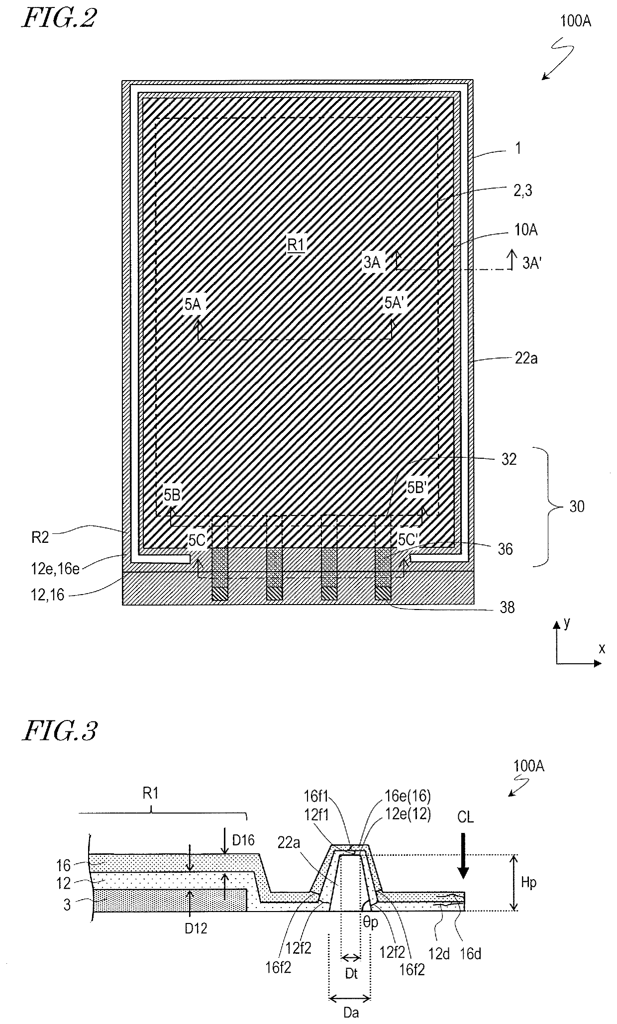
[0048]With reference to FIG. 2 through FIG. 4, a structure of, and a method for producing, the OLED display device 100A according to embodiment 1 of the present invention will be described.

[0049]FIG. 2 is a plan view schematically showing the OLED display device 100A according to an embodiment of the present invention. FIG. 3 is a cross-sectional view schematically showing the OLED display device 100A, and is a cross-sectional view taken along line 3A-3A′ in FIG. 2.

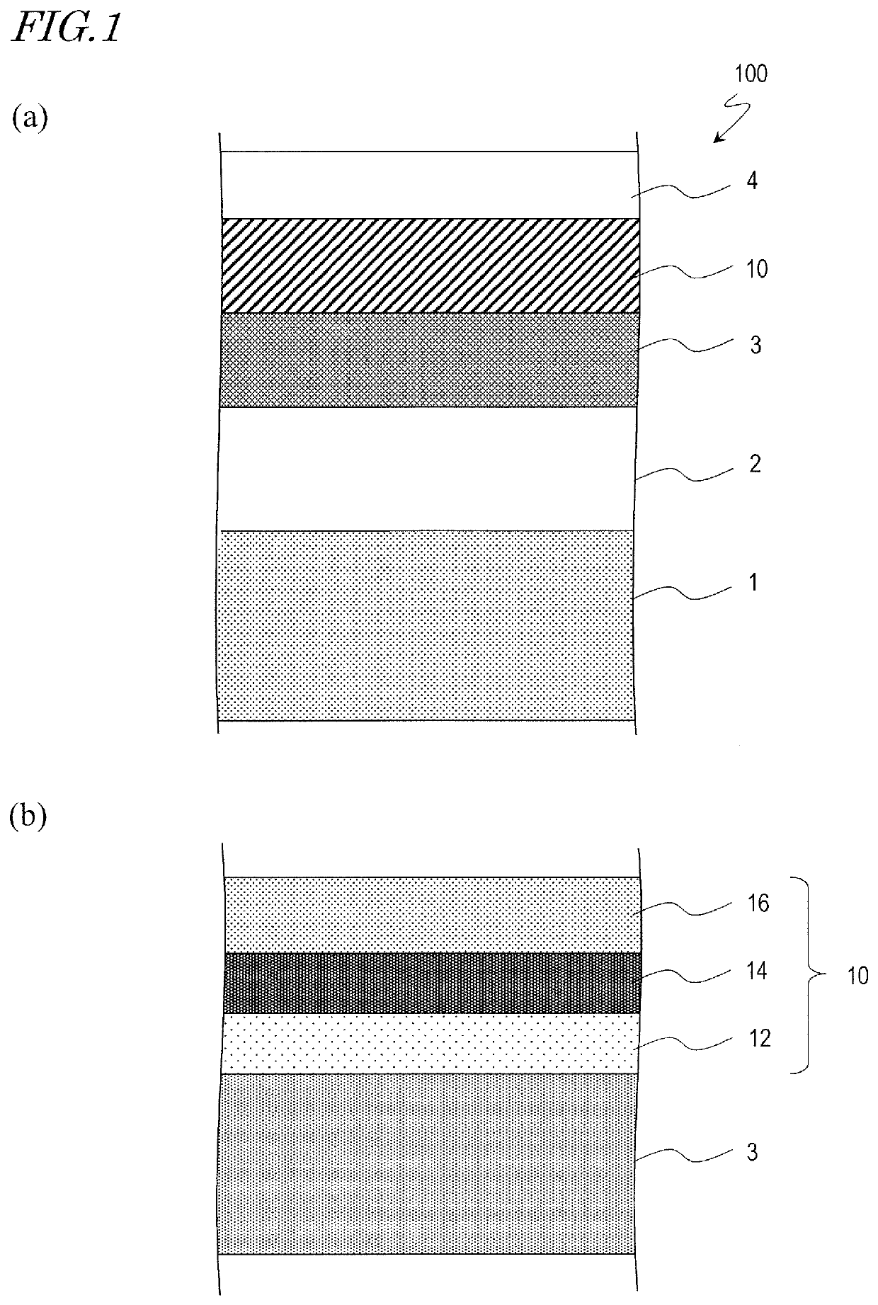
[0050]As shown in FIG. 2, the OLED display device 100A includes the flexible substrate 1, the circuit (back plane) 2 formed on the flexible substrate 1, a plurality of the OLEDs 3 formed on the circuit 2, and a TFE structure 10A formed on the OLEDs 3. A layer including the plurality of OLEDs 3 may be referred to as an “OLED layer 3”. The circuit 2 and the OLED layer 3 may share a part of components. The optional polarizing plate (see reference numeral 4 in FIG. 1) may further be located on the TFE structure 10A. In additi...

embodiment 2

[0118]An OLED display device according to this embodiment is different from the OLED display device according to the above-described embodiment in the structure of the thin film encapsulation structure. The OLED display device according to this embodiment has a feature in the thin film encapsulation structure. The thin film encapsulation structure in this embodiment is applicable to any of the above-described OLED display devices.

[0119]FIG. 12 is a cross-sectional view schematically showing a TFE structure 10B included in an OLED display device according to embodiment 2 of the present invention. In the above-described embodiment, the organic barrier layer 14 included in the TFE structure 10A includes a plurality of solid portions distributed discretely. As shown in FIG. 12, the TFE structure 10B included in the OLED display device according to this embodiment includes a relatively thick organic barrier layer 14 (e.g., an organic barrier layer having a thickness exceeding about 5 μm ...


PUM

PropertyMeasurementUnit
widthaaaaaaaaaa
tapering angleaaaaaaaaaa
thicknessaaaaaaaaaa

Abstract

An organic EL device (100A) includes an active region (R1) including a plurality of organic EL elements and includes a peripheral region (R2) located in a region other than the active region. The organic EL device includes an element substrate (1) including a substrate, and the plurality of organic EL elements supported by the substrate; and a thin film encapsulation structure (10A) covering the plurality of organic EL elements. The thin film encapsulation structure includes a first inorganic barrier layer (12), an organic barrier layer (14) in contact with a top surface of the first inorganic barrier layer, and a second inorganic barrier layer (16) in contact with the top surface of the first inorganic barrier layer and a top surface of the organic barrier layer. The peripheral region includes a first protruding structure (22a) including a portion extending along at least one side of the active region, the first protruding structure being supported by the substrate, and also includes an extending portion (12e), of the first inorganic barrier layer, extending onto the first protruding structure, the first protruding structure having a height larger than a thickness of the first inorganic barrier layer.

Description

TECHNICAL FIELD[0001]The present invention relates to an organic EL device and a method for producing the same.BACKGROUND ART[0002]Organic EL (Electro-Luminescence) display devices start being put into practical use. One feature of an organic EL display device is being flexible. An organic EL display device includes, in each of pixels, at least one organic EL element (Organic Light Emitting Diode: OLED) and at least one TFT (Thin Film Transistor) controlling an electric current to be supplied to each of the at least one OLED. Hereinafter, an organic EL display device will be referred to as an “OLED display device”. Such an OLED display device including a switching element such as a TFT or the like for each of OLEDs is called an “active matrix OLED display device”. A substrate including the TFTs and the OLEDs will be referred to as an “element substrate”.[0003]An OLED (especially, an organic light emitting layer and a cathode electrode material) is easily influenced by moisture to be...

Claims


Application Information

Patent Timeline
Patent Type & Authority Patents(United States)
IPC IPC(8): H01L51/52H01L27/32
CPCH01L51/5253H01L27/3246H01L2227/323H05B33/04H05B33/06H05B33/10H05B33/12H05B33/22G09F9/00G09F9/30H10K59/122H10K59/873H10K59/8722H10K59/8723Y02E10/549H10K50/844H10K59/1201
Inventor KISHIMOTO, KATSUHIKO
Owner SAKAI DISPLAY PROD
Why Eureka
Try Eureka