

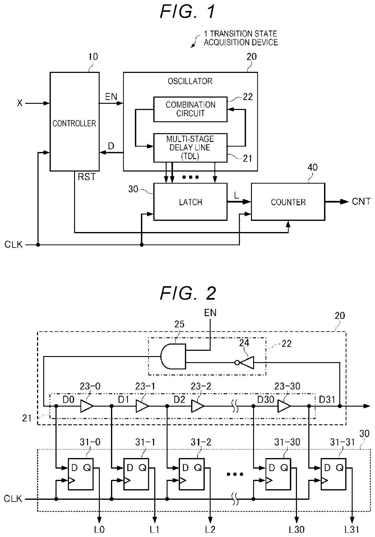
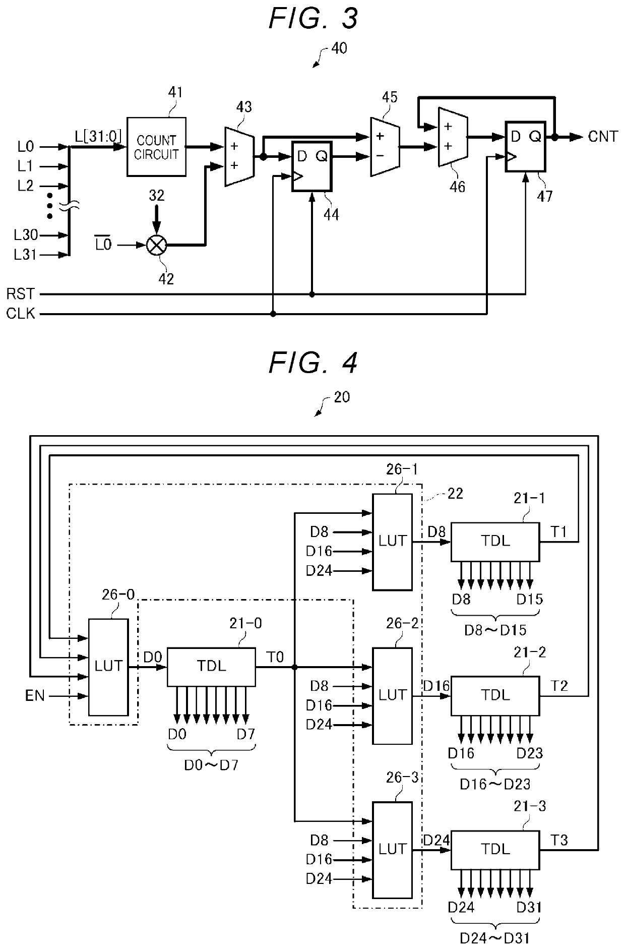
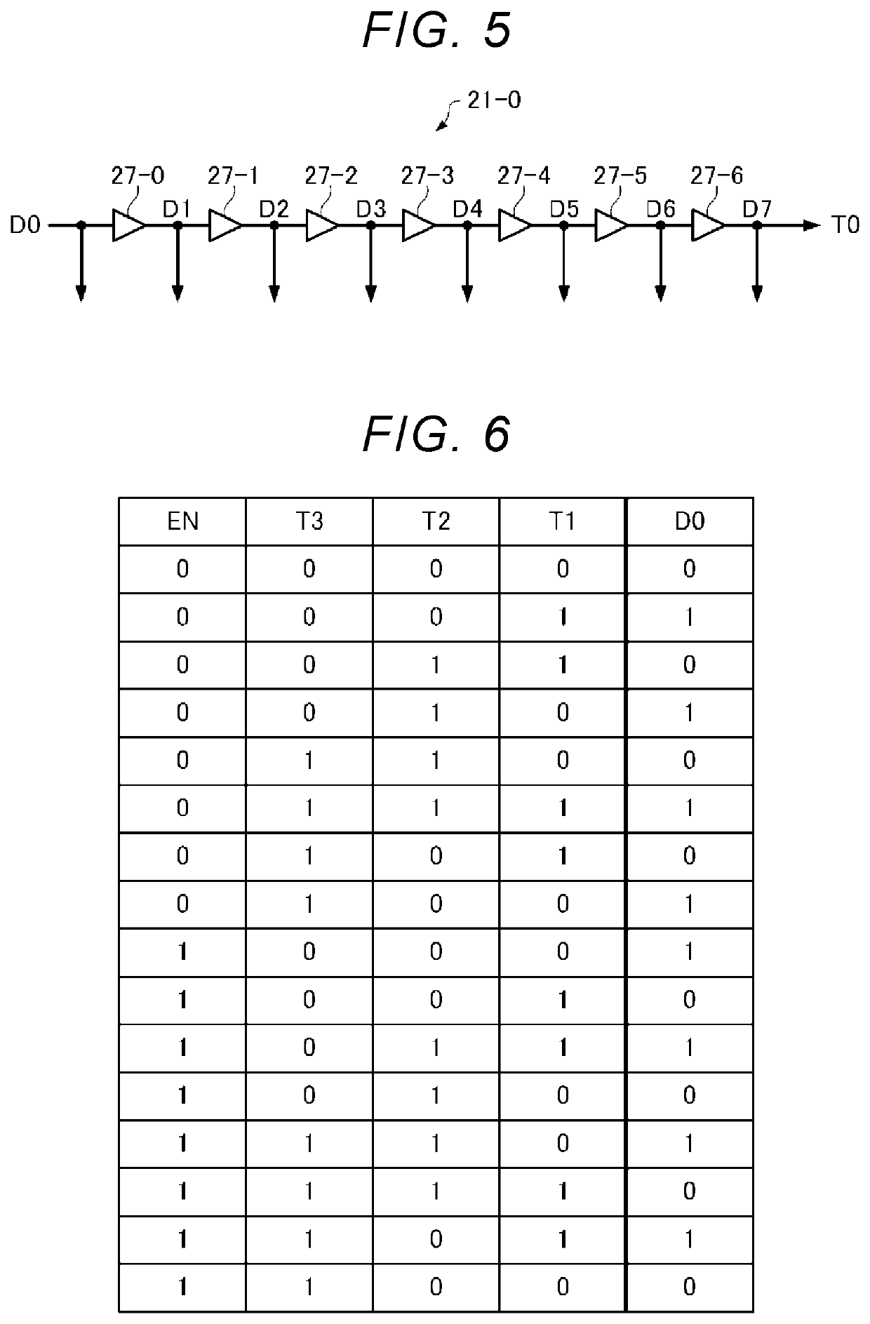
Transition state acquisition device, time-to-digital converter, and A/D conversion circuit
a technology of acquisition device and conversion circuit, which is applied in the direction of horology, automatic control, instruments, etc., can solve problems such as complication
- Summary
- Abstract
- Description
- Claims
- Application Information
AI Technical Summary
Benefits of technology
Problems solved by technology
Method used
Image

Examples
third embodiment
2-3. Third Embodiment
[0171]A third embodiment of the time-to-digital converter 2 generates time-to-digital values TDY1 to TDYm corresponding to at least two time intervals of the time events of a plurality of signals to be measured X similarly to the second embodiment. However, a plurality of transition state acquisition devices 1 are used in the third embodiment of the time-to-digital converter 2.
[0172]FIG. 17 is a diagram showing a configuration in the third embodiment of the time-to-digital converter 2. As shown in FIG. 17, the third embodiment of the time-to-digital converter 2 includes n (n≥2) transition state acquisition devices 1-1 to 1-n and the calculator 3.
[0173]The transition state acquisition devices 1-1 to 1-n start the transition of the state of the tapped delay line 21 based on each of the n signals to be measured X1 to Xn, respectively detect the time events of the signals to be measured X1 to Xn, and respectively output the count values CNT1 to CNTn.
[0174]The calcul...
first embodiment
3-1. First Embodiment
[0183]FIG. 18 is a diagram showing a configuration in a first embodiment of an A / D conversion circuit 100. As shown in FIG. 18, the first embodiment of the A / D conversion circuit 100 includes a reference waveform signal generation circuit 102, a comparator 103, and the time-to-digital converter 2, and converts an input analog signal AIN into a digital signal DOUT and outputs the converted digital signal.
[0184]The reference waveform signal generation circuit 102 generates a reference waveform signal REF based on the reference clock signal CLK. The reference waveform signal REF is a signal whose voltage changes at the same period as that of the reference clock signal CLK, and, for example, may be a triangular wave signal, a ramp wave signal, a sine wave signal, a cosine wave signal, or the like.
[0185]The comparator 103 compares a voltage of the analog signal AIN with a voltage of the reference waveform signal REF generated by the reference waveform signal generati...
second embodiment
3-2. Second Embodiment
[0198]FIG. 21 is a diagram showing a configuration in a second embodiment of the A / D conversion circuit 100. As shown in FIG. 21, the second embodiment of the A / D conversion circuit 100 includes a sample-hold circuit 101, the reference waveform signal generation circuit 102, the comparator 103, and the time-to-digital converter 2, and converts the input analog signal AIN into the digital signal DOUT and outputs the converted digital signal.
[0199]The sample-hold circuit 101 samples and holds a voltage of the analog signal AIN in synchronization with the reference clock signal CLK.
[0200]The reference waveform signal generation circuit 102 generates the reference waveform signal REF based on the reference clock signal CLK. The reference waveform signal REF is the signal whose voltage changes at the same period as that of the reference clock signal CLK, and, for example, may be the triangular wave signal, the ramp wave signal, the sine wave signal, the cosine wave ...
PUM
 Abstract
Description
Claims
Application Information