Storage device and interface chip thereof

a storage device and interface chip technology, applied in the field of flash memory control, can solve the problems of high temperature of the controller, inability to afford such a large throughput, and inability to achieve the effect of ensuring the efficiency and reliability reducing the uncorrectable bit error rate (uber) of the storage device, and increasing the storage capacity of the storage devi

Active Publication Date: 2020-09-01
SILICON MOTION INC (TW)
View PDF22 Cites 2 Cited by
  • Summary
  • Abstract
  • Description
  • Claims
  • Application Information

AI Technical Summary

Benefits of technology

[0004]Another object of the present invention is to provide a storage device and an interface chip thereof to maximize the storage capacity of the storage device while ensuring the efficiency and reliability of the storage device.
[0009]One of the advantages of the present invention is that the interface chip of the present invention increases the storage capacity of the storage device and avoids various problems in the related art. In addition, the interface chip of the present invention can ensure the efficiency and reliability of the storage device. In addition, the interface chip and the storage device of the present invention can perform multi-layer data protection so as to effectively reduce the uncorrectable bit error rate (UBER) of the storage device.

Problems solved by technology

Some problems have arisen in the related art regarding the development of solid state drive (SSD) products with high performance and high durability such as enterprise SSD.
For example, when attempting to increase the storage capacity of an enterprise SSD by increasing the number of flash memory chips in the enterprise SSD, the throughput of a key data path of a controller in the enterprise SSD will greatly increase, but the conventional architecture of the controller is not able to afford such a large throughput.
As the conventional technologies are not able to ensure both performance and reliability at the same time, tradeoffs between the performance and the reliability must be considered.
For another example, the increase of calculation for related data protection can lead to high temperature of the controller.
Therefore, an additional heat dissipation mechanism is required for the controller, wherein the heat dissipation mechanisms will occupy additional space.

Method used


Image

  • Storage device and interface chip thereof
  • Storage device and interface chip thereof
  • Storage device and interface chip thereof

Examples


Embodiment Construction

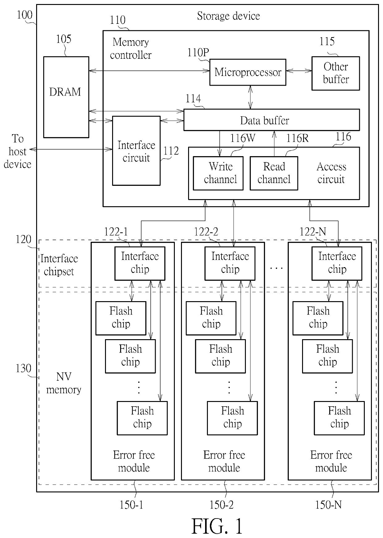
[0021]In the related art, the term “chip” can represent a bare chip (e.g. die) or at least one die protected in a package. For better comprehension, the term “chip” in the present invention can represent a die of an integrated circuit (IC). For example, the term “non-volatile (NV) memory chip” can represent a die of a NV memory IC. For another example, the term “flash chip” can represent a die of a flash memory IC. As another example, the term “interface chip” can represent a die of an interfacing IC. According to some embodiments, one or more chips (such as one or more dice) can be disposed in a package.

[0022]FIG. 1 is a schematic diagram of a storage device 100 according to an embodiment of the present invention. For example, the storage device 100 can be a solid state drive (SSD), such as an enterprise SSD. As shown in FIG. 1, the storage device 100 comprises a Dynamic Random Access Memory (DRAM) 105, a memory controller 110, an interface chipset 120, and a NV memory 130. The mem...


PUM


Abstract

A storage device and an interface chip thereof are provided, wherein the interface chip can be applied to the storage device. The interface chip comprises a slave interface circuit, a master interface circuit, and a control circuit. The storage device comprises a memory controller and a non-volatile (NV) memory, and the NV memory comprises a plurality of NV memory chips. The slave interface circuit is arranged for coupling the interface chip to the memory controller. The master interface circuit is arranged for coupling the interface chip to a set of NV memory chips within the plurality of NV memory chips. A hierarchical architecture in the storage device comprises the memory controller, the interface chip, and the set of NV memory chips. The control circuit is arranged for controlling operations of the interface chip.

Description

BACKGROUND OF THE INVENTION1. Field of the Invention[0001]The present invention relates to flash memory control, and more particularly, to a storage device and an interface chip thereof.2. Description of the Prior Art[0002]Some problems have arisen in the related art regarding the development of solid state drive (SSD) products with high performance and high durability such as enterprise SSD. For example, when attempting to increase the storage capacity of an enterprise SSD by increasing the number of flash memory chips in the enterprise SSD, the throughput of a key data path of a controller in the enterprise SSD will greatly increase, but the conventional architecture of the controller is not able to afford such a large throughput. As the conventional technologies are not able to ensure both performance and reliability at the same time, tradeoffs between the performance and the reliability must be considered. For another example, the increase of calculation for related data protect...

Claims


Application Information

Patent Timeline
Patent Type & Authority Patents(United States)
IPC IPC(8): G06F13/16G06F11/10G11C29/52
CPCG06F11/1004G06F11/1068G06F13/1668G06F11/1012G06F11/108G11C29/52G06F13/1673
Inventor YANG, TSUNG-CHIEH
Owner SILICON MOTION INC (TW)
Why Eureka
Try Eureka