Method of manufacturing FinFET with reduced parasitic capacitance and FinFET structure formed thereby
a technology of parasitic capacitance and finfet structure, which is applied in the direction of semiconductor devices, electrical apparatus, transistors, etc., can solve the problems of reducing chip performance, increasing ic's effective capacitance, and providing no other device performance benefi
- Summary
- Abstract
- Description
- Claims
- Application Information
AI Technical Summary
Benefits of technology
Problems solved by technology
Method used
Image

Examples
Embodiment Construction
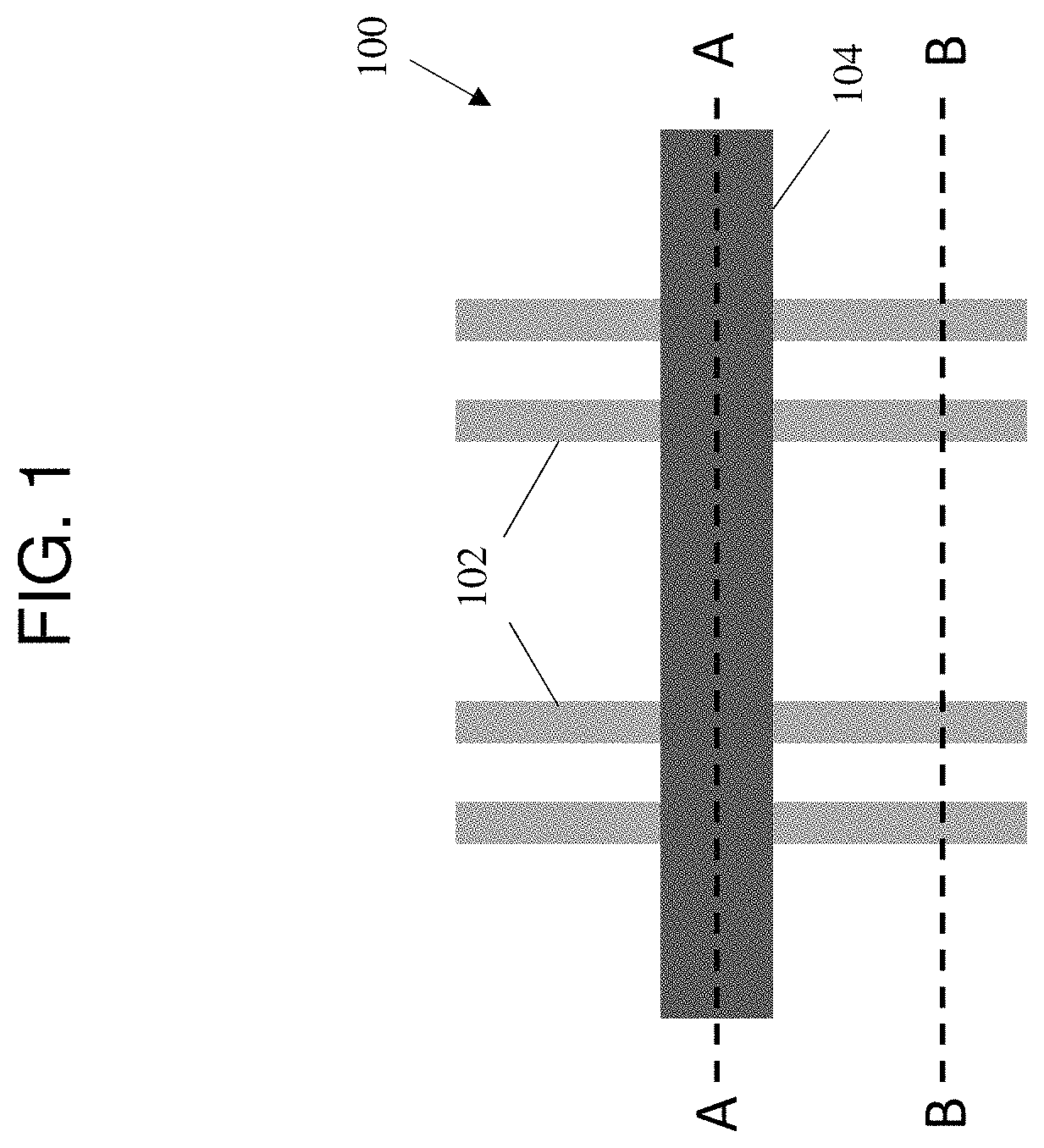
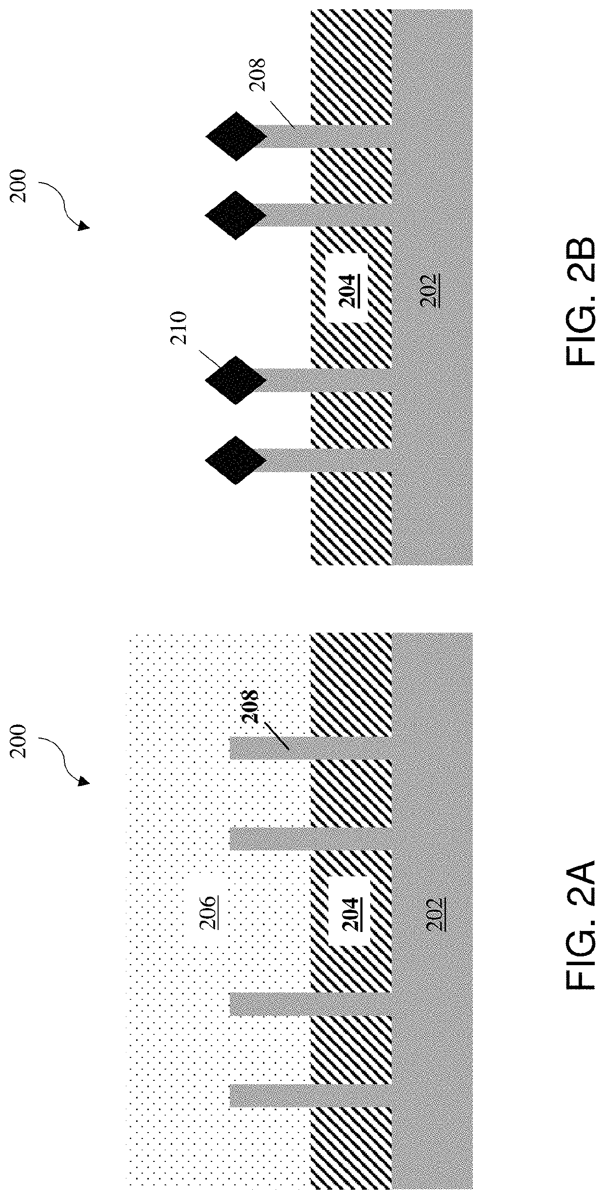
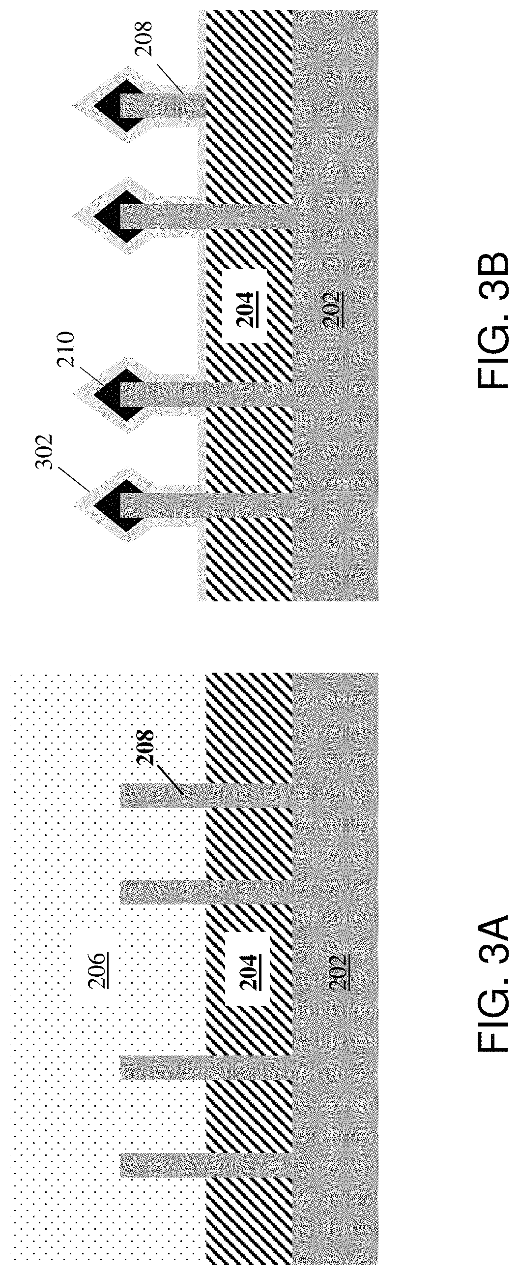
[0019]The subject matter disclosed herein relates to methods of manufacturing FinFETs. More specifically, various aspects described herein relate to methods of manufacturing FinFETs with reduced contact-to-gate parasitic capacitance, and FinFET structures formed thereby.
[0020]As noted above, in conventional scaled down FinFETs (such as 7 nm and beyond), excessive recess depths of the trench silicide (TS) contact can generate excessive parasitic capacitance to a nearby gate which can significantly increase an IC's effective capacitance and degrade chip performance while providing no other device performance benefit. In contrast to convention, various aspects of the disclosure include methods of manufacturing FinFETs which prevent excessive depth of the TS contact and thereby reduce contact-to-gate parasitic capacitance. In other aspects of the disclosure, FinFET devices are formed that allow for reduced contact-to-gate parasitic capacitance which in turn allows for reduced effective ...
PUM
| Property | Measurement | Unit |
|---|---|---|
| distance | aaaaa | aaaaa |
| thickness | aaaaa | aaaaa |
| depth/thickness | aaaaa | aaaaa |
Abstract
Description
Claims
Application Information
 - Generate Ideas
- Intellectual Property
- Life Sciences
- Materials
- Tech Scout
- Unparalleled Data Quality
- Higher Quality Content
- 60% Fewer Hallucinations
Browse by: Latest US Patents, China's latest patents, Technical Efficacy Thesaurus, Application Domain, Technology Topic, Popular Technical Reports.
© 2025 PatSnap. All rights reserved.Legal|Privacy policy|Modern Slavery Act Transparency Statement|Sitemap|About US| Contact US: help@patsnap.com