
Substrate comprising plurality of signal lines and electronic device comprising same

a technology of signal lines and substrates, which is applied in the direction of cross-talk/noise/interference reduction, flexible printed circuits, high-frequency circuit adaptations, etc., can solve the problems of electro magnetic interference (emi) phenomenon, and achieve the improvement of data transmission/reception rate between the transmitting side and the receiving side, and the acquisition of signal integrity

Active Publication Date: 2020-11-03
SAMSUNG ELECTRONICS CO LTD
View PDF14 Cites 1 Cited by
  • Summary
  • Abstract
  • Description
  • Claims
  • Application Information

AI Technical Summary

Benefits of technology

[0008]According to one embodiment of the present invention, since a transmitting side transmits differential signals of data to transmit to a receiving side through three signal lines installed on a circuit board or substrate and the receiving side obtains the data by processing (e.g., processing the differential signals or calculating the differential signals) transmitted through the three signal lines (e.g., a first signal line, a second signal line and a third signal line), a data transmission / reception rate between the transmitting side and the receiving side may be improved. According to various embodiments of the present invention, since impedance formed between the first signal line and the second signal line, impedance formed between the first signal line and the third signal line, and impedance formed between the second signal line and the third signal line are designed substantially the same, electro magnetic interference between the signal lines may be improved and signal integrity may be also acquired. According to various embodiments of the present invention, since the three signal lines provided to transmit the differential signals are arranged, when viewed from a cross section of the substrate, substantially in a triangle shape in which other two signal lines are symmetrically disposed on both sides of one signal lines, a wiring space of the signal lines of the board or substrate and / or a size of the substrate may be reduced.

Problems solved by technology

An electric field may be generated due to current flow at the signal line through which the data is transmitted, and such an electric field may cause an electro magnetic interference (EMI) phenomenon by loading noise in a signal transmitted on other adjacent signal line.

Method used


Image

  • Substrate comprising plurality of signal lines and electronic device comprising same
  • Substrate comprising plurality of signal lines and electronic device comprising same
  • Substrate comprising plurality of signal lines and electronic device comprising same

Examples


Embodiment Construction

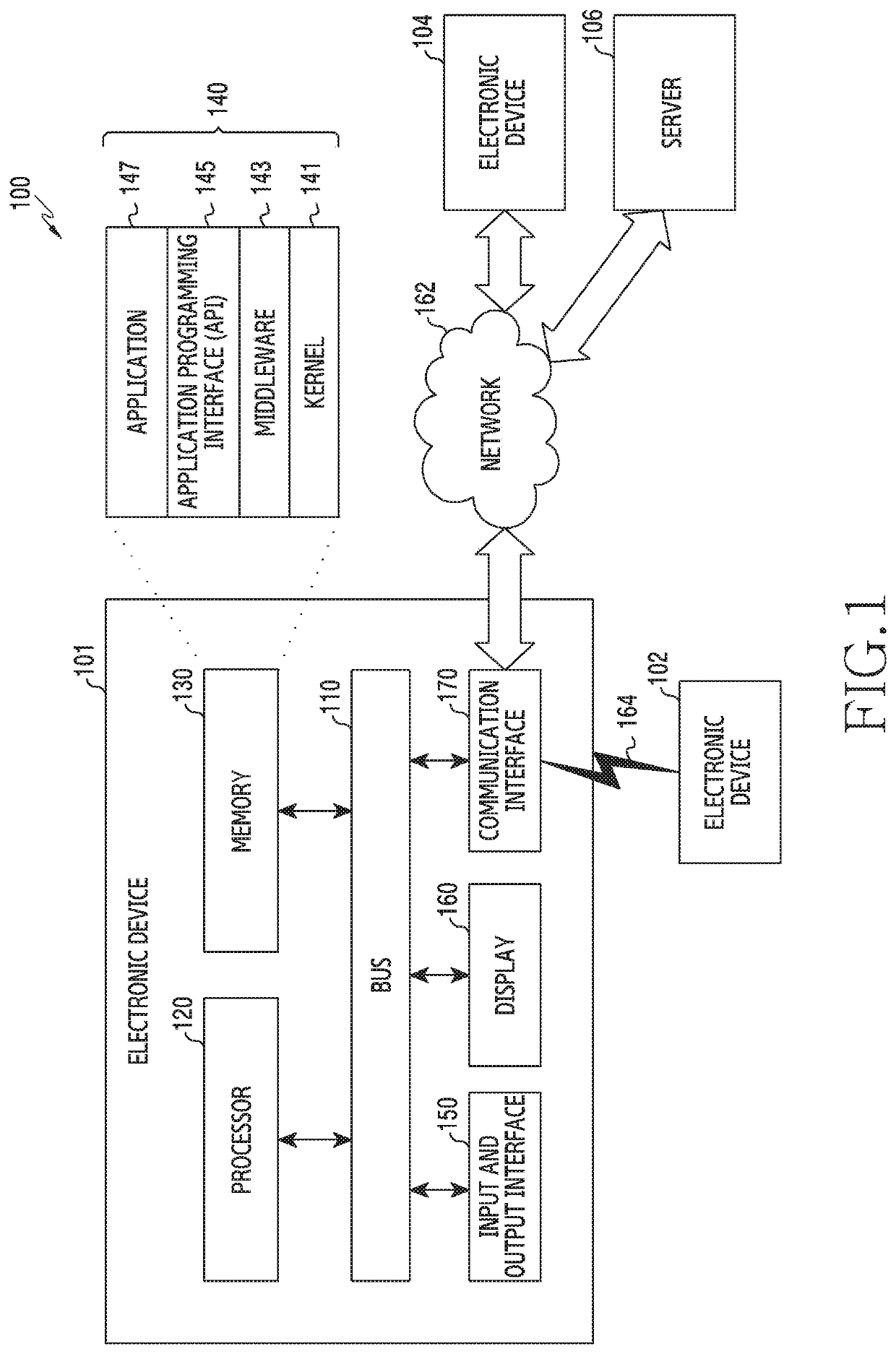
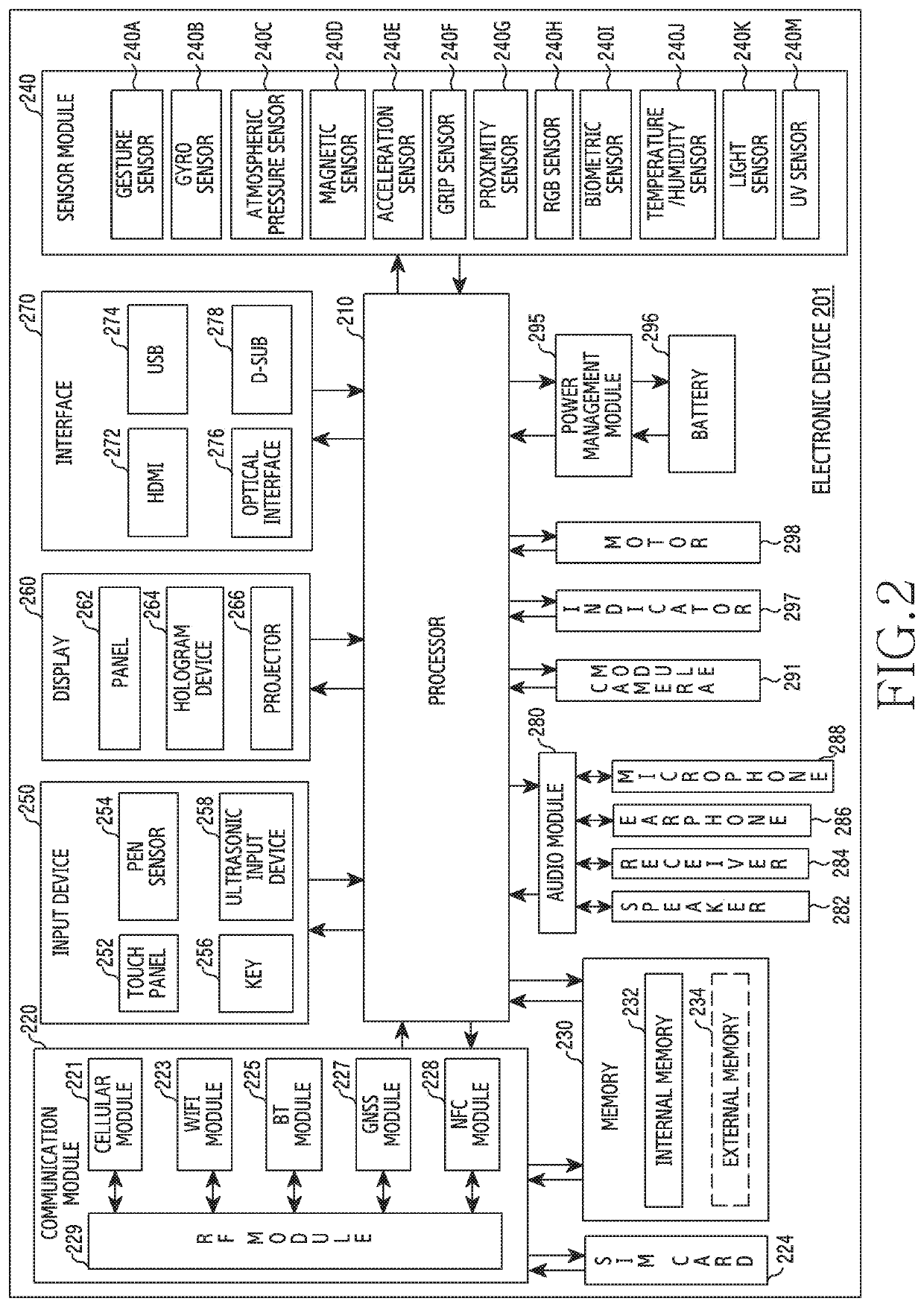
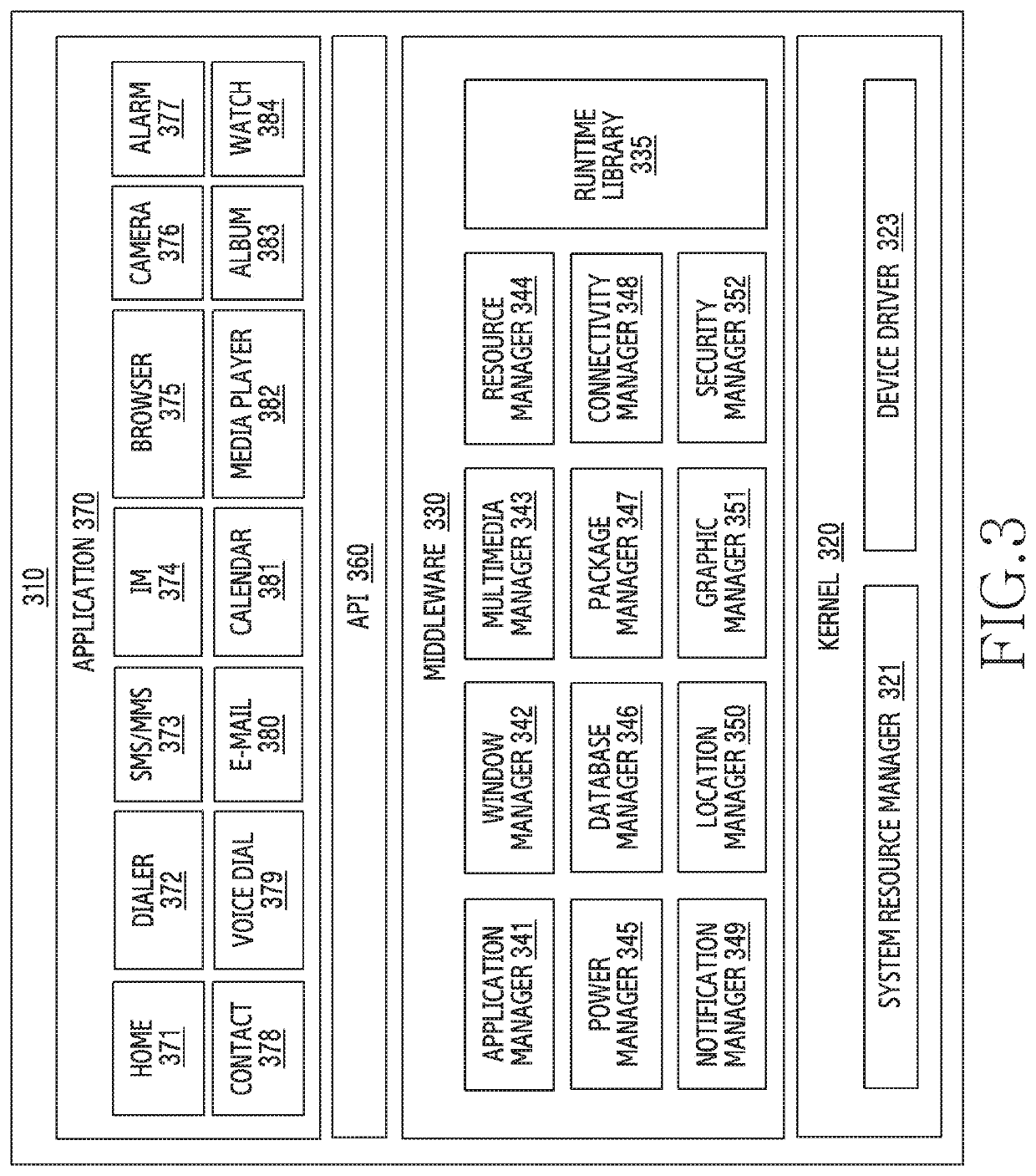
[0020]Hereinafter, various embodiments of the present disclosure will be described with reference to the accompanying drawings. However, it should be understood that there is no intent to limit the present disclosure to the particular forms disclosed herein; rather, the present disclosure should be construed to cover various modifications, equivalents, and / or alternatives of embodiments of the present disclosure. In describing the drawings, similar reference numerals may be used to designate similar constituent elements. Singular forms may include plural forms as well unless the context clearly indicates otherwise. In the present disclosure, the expression “A or B” or “at least one of A or / and B” may include all possible combinations of the items listed. The expression “a first”, “a second”, “the first”, or “the second” used in various embodiments of the present disclosure may modify various components regardless of the order and / or the importance but does not limit the correspondin...


PUM


Abstract

The present disclosure relates to a 5th generation (5G) or pre-5G communication system for supporting a higher data transmission rate than 4th generation (4G) communication systems such as long term evolution (LTE). In a wireless communication system, a transmission apparatus comprises at least one antenna port for transmitting / receiving a signal, an analogue filter for selecting the frequency of the signal, and a voltage standing wave ratio (VSWR) detection unit for measuring the VSWR of the antenna port, wherein the VSWR detection unit is configured to detect both a forward signal and a reverse signal for an input terminal of the analogue filter, to determine the respective power values of a forward signal and a reverse signal for an output terminal of the analogue filter by applying characteristic parameters of the analogue filter to the detected forward signal and reverse signal, and to determine the VSWR of the antenna port on the basis of the respective power values of the forward signal and the reverse signal for the output terminal of the analogue filter.

Description

TECHNICAL FIELD[0001]Various embodiments of the present invention relate to a substrate including a plurality of signal lines and an electronic device including the same.BACKGROUND ART[0002]An electronic device is provided in various forms such as a smart phone, a tablet personal computer (PC), a personal digital assistant (PDA) with development of digital technology. The electronic device is also developed in a form wearable on a user so as to improve portability and user's accessibility.[0003]The electronic device may include a printed circuit board (PCB) which sets an execution environment of the electronic device, maintains its information, and supports data input / output and exchange of components. The PCB may include signal lines for transmitting or receiving data between electronic parts. An electric field may be generated due to current flow at the signal line through which the data is transmitted, and such an electric field may cause an electro magnetic interference (EMI) ph...

Claims


Application Information

Patent Timeline
Patent Type & Authority Patents(United States)
IPC IPC(8): H05K1/11H05K1/02
CPCH05K1/115H05K1/024H05K1/0245H05K2201/05H05K2201/0195H05K1/025H05K1/0218
Inventor KIM, MAN-HOSHIM, JONG-WANJUNG, HWA JOONGKIM, TAE-YUNCHOI, YONGHWANLEE, KIHUK
Owner SAMSUNG ELECTRONICS CO LTD
Learn More