
Method for manufacturing nonreciprocal circuit device and method for manufacturing composite electronic component

a non-reciprocal circuit and electronic component technology, applied in the direction of printed circuit assembling, printed circuit manufacturing, waveguide type devices, etc., can solve the problems of large distance between the ferrite-magnet device and other devices, leakage of magnetic flux of permanent magnets, and large distance required for miniaturization

Active Publication Date: 2011-05-10
MURATA MFG CO LTD
View PDF14 Cites 0 Cited by
  • Summary
  • Abstract
  • Description
  • Claims
  • Application Information

AI Technical Summary

Benefits of technology

The present invention provides methods for manufacturing nonreciprocal circuit devices and composite electronic components that can be smaller in size. These methods eliminate the influence of the magnetic force of the permanent magnet in the ferrite-magnet device, making it easier to miniaturize the device. By using a plate made of magnetic material on the back surface of the substrate, magnetic interference with other devices bonded to the substrate is reduced, allowing the devices to be arranged closer to the ferrite-magnet device. This results in a smaller nonreciprocal circuit device or composite electronic component.

Problems solved by technology

Therefore, a leakage magnetic flux of the permanent magnet which has already been magnetized tends to attract or repel other devices which are bonded to the surface of the substrate at the same time and which have magnetic portions.
Consequently, a large distance is required between the ferrite-magnet device and other devices.
Thus, there is a problem in that the size of a nonreciprocal circuit device or a composite electronic component provided with the ferrite-magnet device is large, and cannot be sufficiently reduced.

Method used


Image

  • Method for manufacturing nonreciprocal circuit device and method for manufacturing composite electronic component
  • Method for manufacturing nonreciprocal circuit device and method for manufacturing composite electronic component
  • Method for manufacturing nonreciprocal circuit device and method for manufacturing composite electronic component

Examples


first preferred embodiment

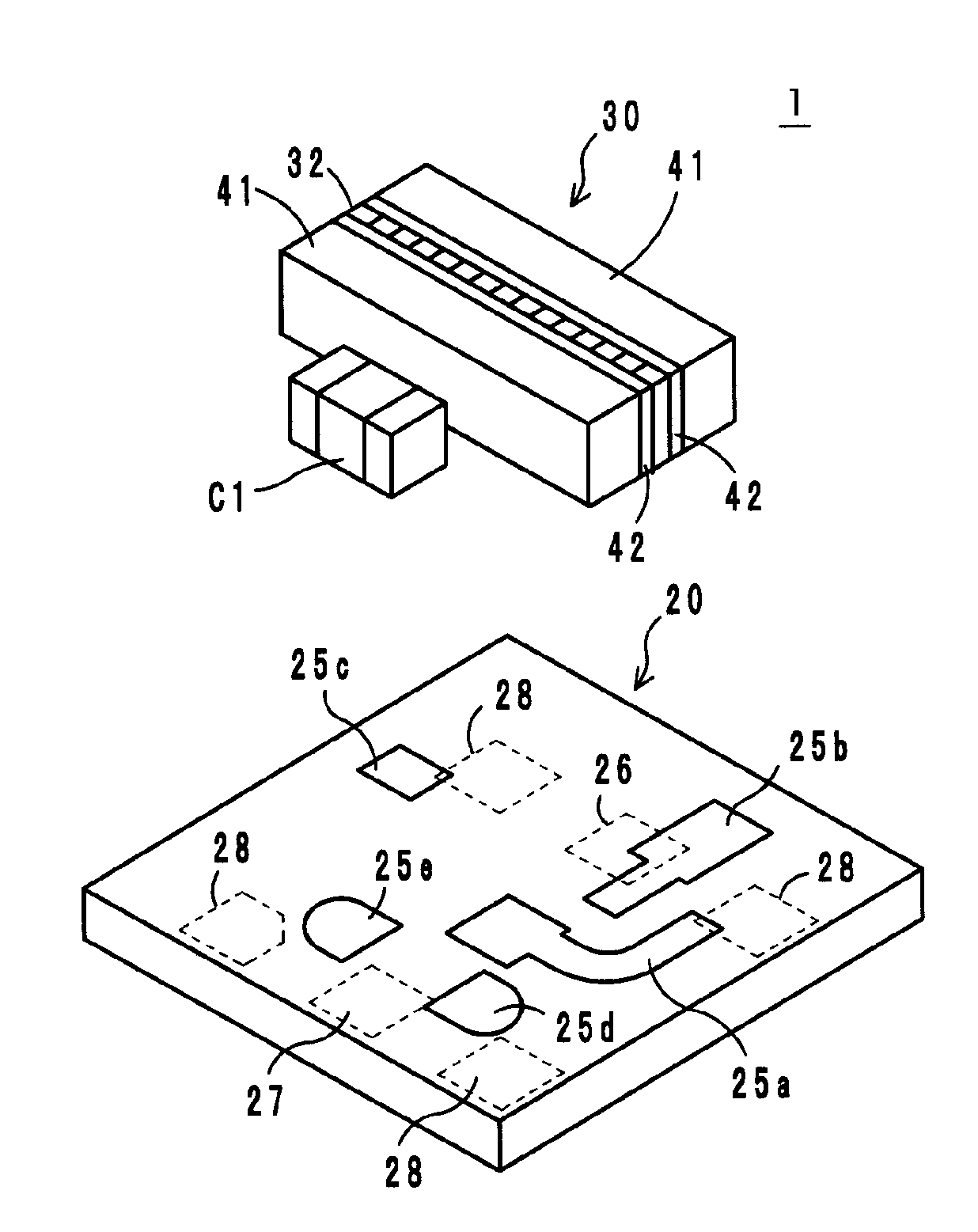
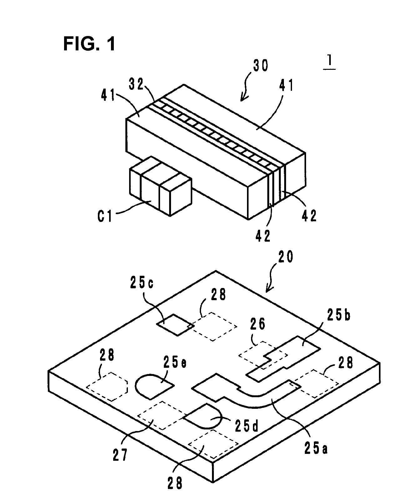
[0029]FIG. 1 is an exploded perspective view of a two-port type isolator 1 in a first preferred embodiment of the present invention. This two-port type isolator 1 is a lumped-constant isolator and includes a substrate 20, a ferrite-magnet device 30 composed of ferrite 32, and a pair of permanent magnets 41, and a capacitor C1 defining a portion of a matching circuit device.

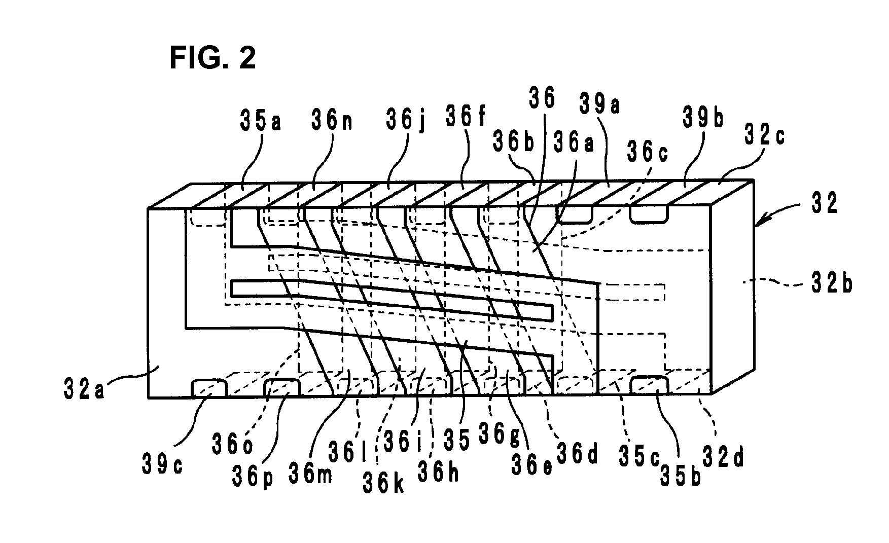
[0030]As shown in FIG. 2, the ferrite 32 is provided with a first center electrode 35 and a second center electrode 36 electrically insulated from each other on front and back principal surfaces 32a and 32b. Here, the ferrite 32 preferably has a substantially rectangular shape having a first principal surface 32a and a second principal surface 32b opposite and parallel or substantially parallel to each other.

[0031]The permanent magnets 41 are preferably bonded to the principal surfaces 32a and 32b with, for example, an epoxy adhesive 42 therebetween so as to apply a direct current magnetic field to the ferrite 32 ...

second preferred embodiment

[0052]FIG. 10 is an exploded perspective view of a two-port type isolator 2 according to a second preferred embodiment of the present invention. This two-port type isolator 2 has substantially the same configuration as that of the above-described first preferred embodiment and a difference is that all of the matching circuit devices C1, C2, CS1, CS2, and R are chip type devices that are soldered to the surface of a printed circuit board 20A. The surface of the printed circuit board 20A is provided with terminal electrodes 25d and 25e arranged to connect individual matching circuit devices, in addition to the terminal electrodes 25a, 25b, and 25c arranged to connect both ends of the first and the second center electrodes 35 and 36. Furthermore, input and output electrodes and a ground electrode are also provided, although not shown in the drawing.

[0053]In production of the isolator 2, the magnetic plate 50 (refer to FIG. 7B) is disposed on the back surface of the substrate 20A and re...

third preferred embodiment

[0054]FIG. 11 shows a composite electronic component 3 according to a third preferred embodiment of the present invention. This composite electronic component 3 defines a module by mounting the above-described isolator 2 and a power amplifier 81 on the surface of a printed circuit board 82. Necessary chip circuit devices 83a to 83f are also mounted around the power amplifier 81.

[0055]FIG. 12 shows a circuit configuration of the composite electronic component 3. The output of an impedance matching circuit 86 is input into the high frequency power amplifier circuit 81, and the output thereof is input into the isolator 2 through an impedance matching circuit 85.

[0056]In the production process of the composite electronic component 3, the magnetic plate 50 (refer to FIG. 7B) is disposed on the back surface of the substrate 82 and reflow-soldering of the ferrite-magnet device 30, the power amplifier 81, and the various matching circuit devices to the surface of the substrate 82 is perform...


PUM

PropertyMeasurementUnit
distanceaaaaaaaaaa
distanceaaaaaaaaaa
distanceaaaaaaaaaa

Abstract

A method for manufacturing a nonreciprocal circuit device in which a ferrite-magnet device including ferrite having first and second center electrodes arranged to intersect and be electrically insulated from each other and a pair of permanent magnets fixed to both principal surfaces of the ferrite so as to apply a direct current magnetic field to the ferrite is solder-bonded to a surface of a substrate. The ferrite-magnet device is solder-bonded to the surface of the substrate while a magnetic plate is disposed on a back surface of the substrate.

Description

BACKGROUND OF THE INVENTION[0001]1. Field of the Invention[0002]The present invention relates to a method for manufacturing a nonreciprocal circuit device, and in particular, to a nonreciprocal circuit device, e.g., an isolator or a circulator, which is used in a microwave band and a method for manufacturing a composite electronic component including the nonreciprocal circuit device.[0003]2. Description of the Related Art[0004]Nonreciprocal circuit devices, e.g., isolators and circulators, have a characteristic that signals are transmitted in a predetermined specific direction and are not transmitted in the reverse direction. For example, the isolator is used in transmitting circuit portions of mobile communication equipment, e.g., automobile telephones and cellular phones, by taking advantage of this characteristic.[0005]Generally, this type of nonreciprocal circuit device includes a ferrite-magnet device made of ferrite provided with a center electrode and a permanent magnet arran...

Claims


Application Information

Patent Timeline
Patent Type & Authority Patents(United States)
IPC IPC(8): H01P11/00H01Q13/00H01Q17/00H01L21/00H01L23/48H01S4/00
CPCH01P1/387H01P11/00Y10T29/49144Y10T29/49018Y10T29/49002Y10T29/49016Y10T29/4913
Inventor TAGUCHI, YOSHINORI
Owner MURATA MFG CO LTD
Learn More