Organic light-emitting diode display device

a technology of light-emitting diodes and display devices, which is applied in the direction of instruments, static indicating devices, etc., can solve the problems of increasing the cost of circuit components and time loss, and achieve the effect of simplifying the configuration of external compensation circuits and reducing compensation tim

Active Publication Date: 2020-11-24
LG DISPLAY CO LTD
View PDF38 Cites 0 Cited by
  • Summary
  • Abstract
  • Description
  • Claims
  • Application Information

AI Technical Summary

Benefits of technology

[0011]An object of the present invention is to provide an OLED display device capable of simplifying the configuration of an external compensation circuit and reducing a compensation time.

Problems solved by technology

However, the OLED display device having a conventional external compensation function requires an additional panel sensing time for the external compensation operation at a power-ON / OFF time during the manufacturing process and real-time driving and additionally requires a sensing circuit and an operation circuit for acquiring the compensation values and the memory for storing the compensation values, thereby causing time loss and increasing cost of circuit components.

Method used


Image

  • Organic light-emitting diode display device
  • Organic light-emitting diode display device
  • Organic light-emitting diode display device

Examples


Embodiment Construction

[0040]Reference will now be made in detail to the exemplary embodiments of the present invention, examples of which are illustrated in the accompanying drawings. Wherever possible, the same reference numbers will be used throughout the drawings to refer to the same or like parts.

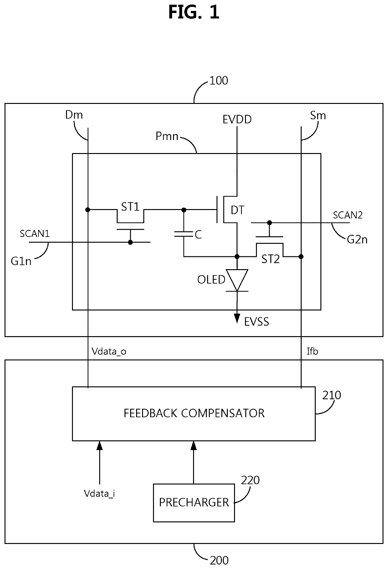
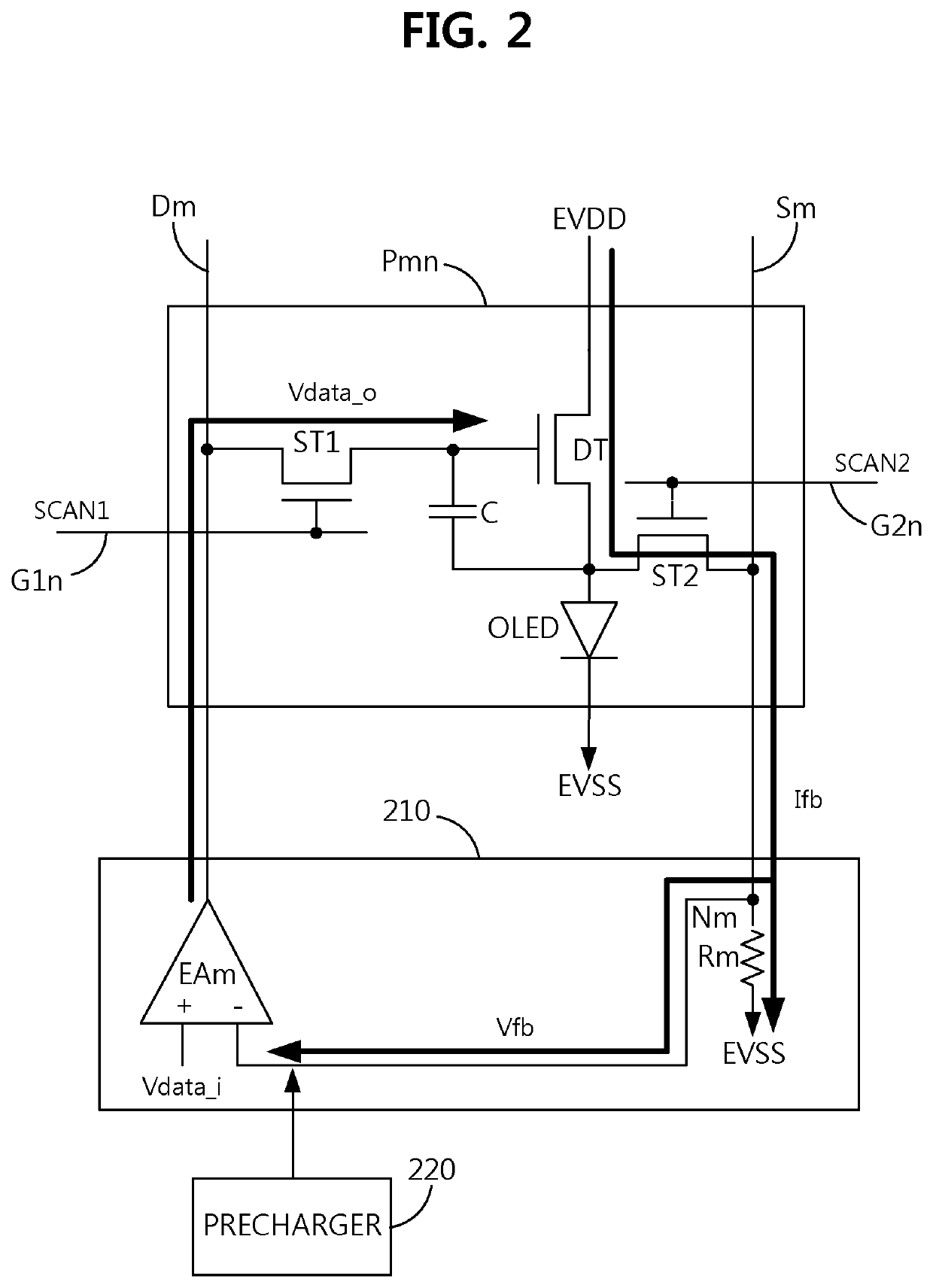
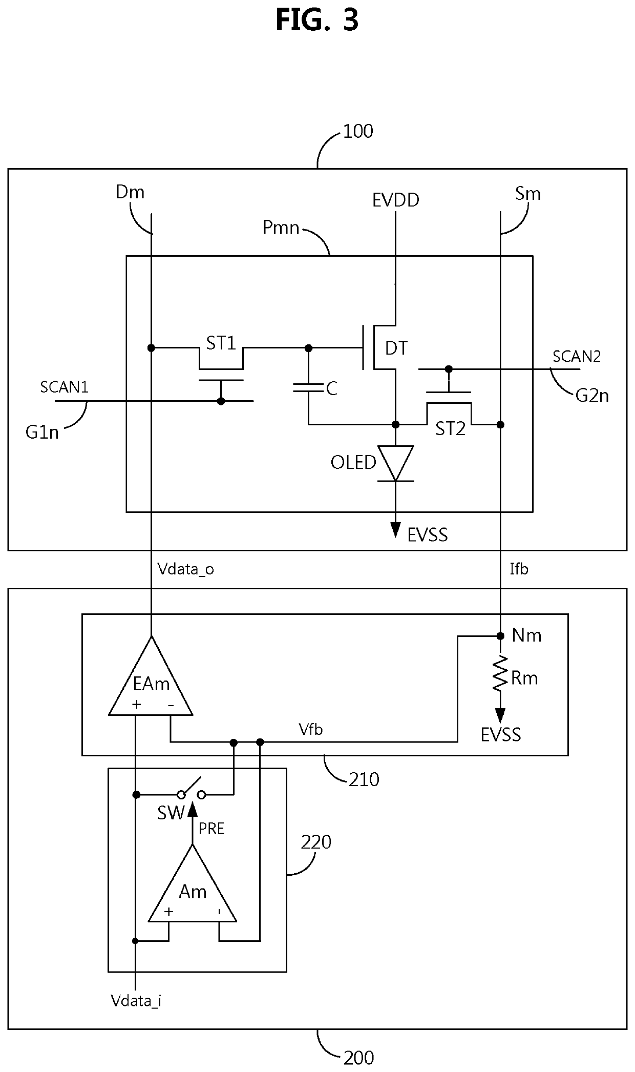
[0041]FIG. 1 is a circuit diagram illustrating a partial configuration of an OLED display device according to an embodiment of the present invention and FIG. 2 is a diagram illustrating an operation of a pixel shown in FIG. 1.

[0042]Referring to FIG. 1, the OLED display device according to an embodiment includes a display panel 100 and a data driver 200. The display panel 100 representatively shows an (m, n)-th pixel Pmn located in an m-th (where m is a natural number) pixel column and an n-th (where n is a natural number) pixel row, among a plurality of pixels configured in the form of a matrix. The data driver 200 representatively shows an m-th feedback compensator circuit 210 connected as a feedback struct...


PUM

PropertyMeasurementUnit
feedback voltageaaaaaaaaaa
voltageaaaaaaaaaa
precharge voltageaaaaaaaaaa

Abstract

An OLED display device capable of simplifying the configuration of an external compensation circuit and reducing a compensation time is disclosed. The OLED display device includes a display panel including a pixel, a feedback compensator circuit connected to the pixel through a data line and a sensing line of the display panel, the feedback compensator circuit including an error amplifier configured to receive, through a feedback line, a feedback current flowing into the sensing line and a feedback voltage generated by a sensing resistor, from the pixel during a scan period, compare a data input voltage with the feedback voltage to adjust a data output voltage supplied to the pixel through the data line, and set a target current for driving an OLED element in the pixel, and a precharger configured to precharge the feedback compensator circuit at a front part of the scan period.

Description

CROSS-REFERENCE TO RELATED APPLICATIONS[0001]This application claims the benefit of Republic of Korea Patent Application No. 10-2016-0184071, filed on Dec. 30, 2016, which is hereby incorporated by reference in its entirety.BACKGROUND OF THE INVENTIONField of the Invention[0002]The present invention relates to an organic light-emitting diode (LED) display device for simplifying the configuration of an external compensation circuit and reducing a compensation time.Discussion of the Related Art[0003]A representative flat panel display device for displaying images using digital data includes a liquid crystal display (LCD) using liquid crystal, an organic light-emitting diode (OLED) display device using OLEDs, and an electrophoretic display (EPD) using electrophoretic particles.[0004]Thereamong, the OLED display device is a self-luminescent device which causes an organic light-emitting layer to emit light through recombination of electrons and holes and is expected as a next-generation ...

Claims


Application Information

Patent Timeline
Patent Type & Authority Patents(United States)
IPC IPC(8): G09G3/3233G09G3/3275G09G3/3266
CPCG09G3/3266G09G3/3233G09G3/3275G09G2300/0861G09G2310/08G09G2310/0262G09G2310/0251G09G2310/0248G09G2330/08G09G2330/021G09G2320/0233G09G2320/0252G09G2320/0295G09G2310/0291G09G2320/043G09G2310/0297G09G2330/028G09G2320/0693G09G3/3291G09G2300/0842G09G2300/043G09G2230/00G09G2300/0828
Inventor KWON, YONG-CHULKIM, JANG-HWANPARK, DONG-WONPARK, JONG-MINLEE, JOON-HEE
Owner LG DISPLAY CO LTD
Why Eureka
Try Eureka