Method of fabricating a semiconductor device

a semiconductor and semiconductor technology, applied in the field of semiconductor devices and a method of fabricating semiconductor devices, can solve the problems of damage to the suspended portion and inability to thoroughly remove the photoresist layer, and achieve the effects of high liquid spray pressure, increased lift-off spray pressure, and increased pressur

Active Publication Date: 2020-12-29
SEMICON MFG ELECTRONICS (SHAOXING) CORP
View PDF3 Cites 2 Cited by
  • Summary
  • Abstract
  • Description
  • Claims
  • Application Information

AI Technical Summary

Benefits of technology

[0010]It is an objective of the present invention to solve the above-described problem with the conventional method, i.e., easy damage to a suspended portion of a passivation layer by presenting a method of fabricating a semiconductor device.
[0033]In the method provided in the present invention, after the upper electrode layer is formed, the sacrificial portion is formed at the first end of the upper electrode layer, and the passivation layer covers both the upper electrode layer and the sacrificial portion so that the passivation layer is supported at a corresponding end by the sacrificial portion and is not suspended at all. As a result, the passivation layer is able to withstand a larger pressure and will not be damaged at said end portion in a subsequent process.
[0034]For example, the passivation layer is able to withstand a high liquid spray pressure without breakage during a lift-off process for forming the contact pad and allows an even higher lift-off spray pressure during the removal of photoresist. This enables increased photoresist lift-off efficiency and mitigates the problem of incomplete photoresist removal. In addition, during the lift-off process, no photoresist will be filled under the passivation layer because it is not suspended at all. This additionally mitigates the problem of incomplete photoresist removal.

Problems solved by technology

However, when acting on the passivation layer 50, such a high spray pressure may cause damage to the suspended portion 51.
This is usually avoided by using a lower spay pressure, which, however, may be not able to thoroughly remove the photoresist layer.

Method used


Image

  • Method of fabricating a semiconductor device
  • Method of fabricating a semiconductor device
  • Method of fabricating a semiconductor device

Examples


Embodiment Construction

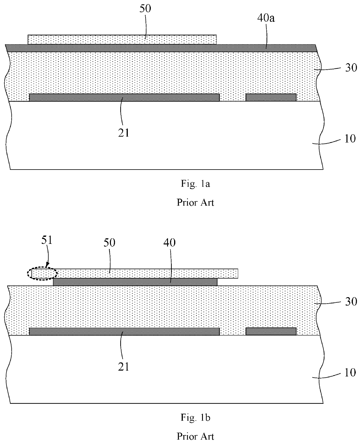
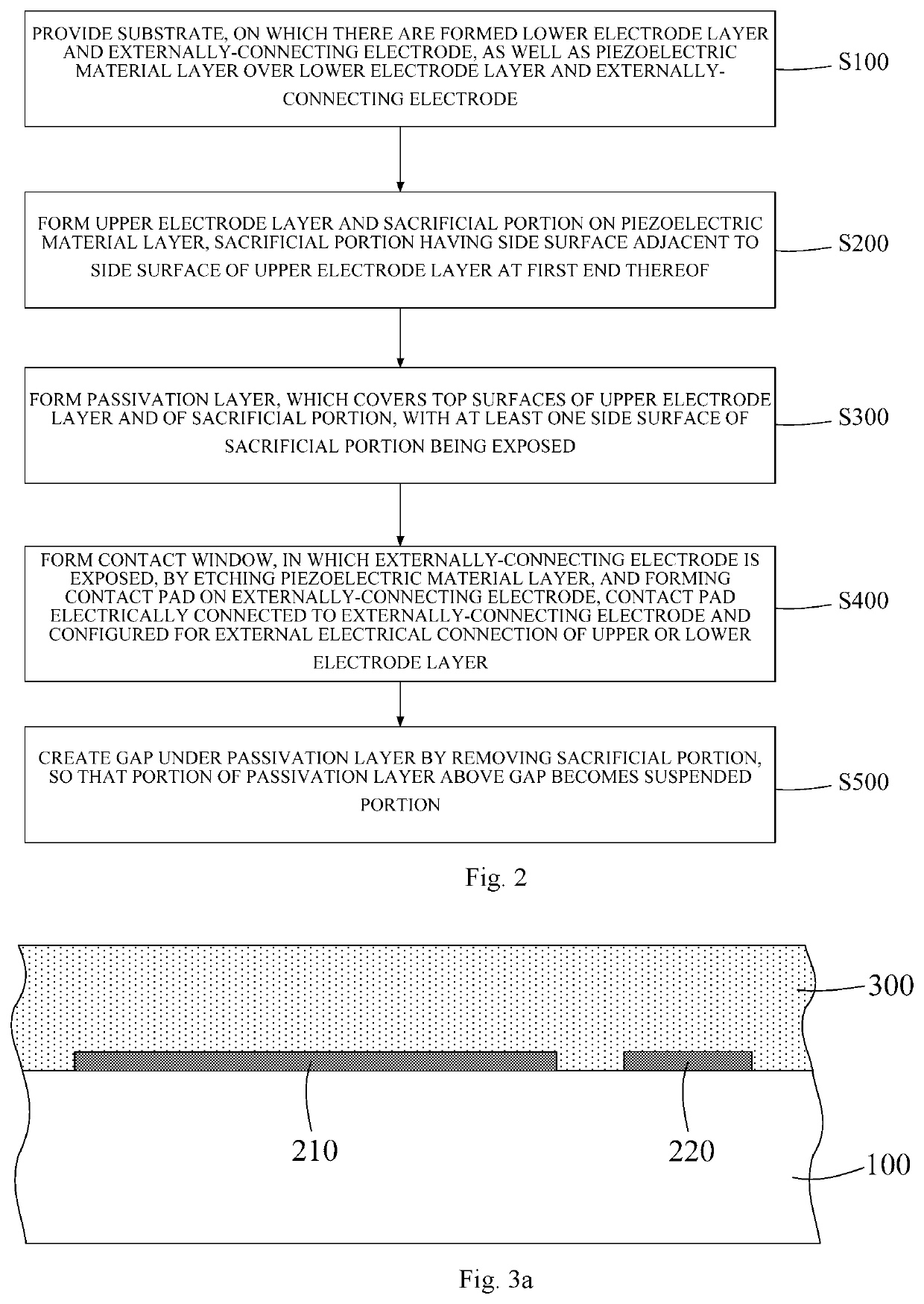
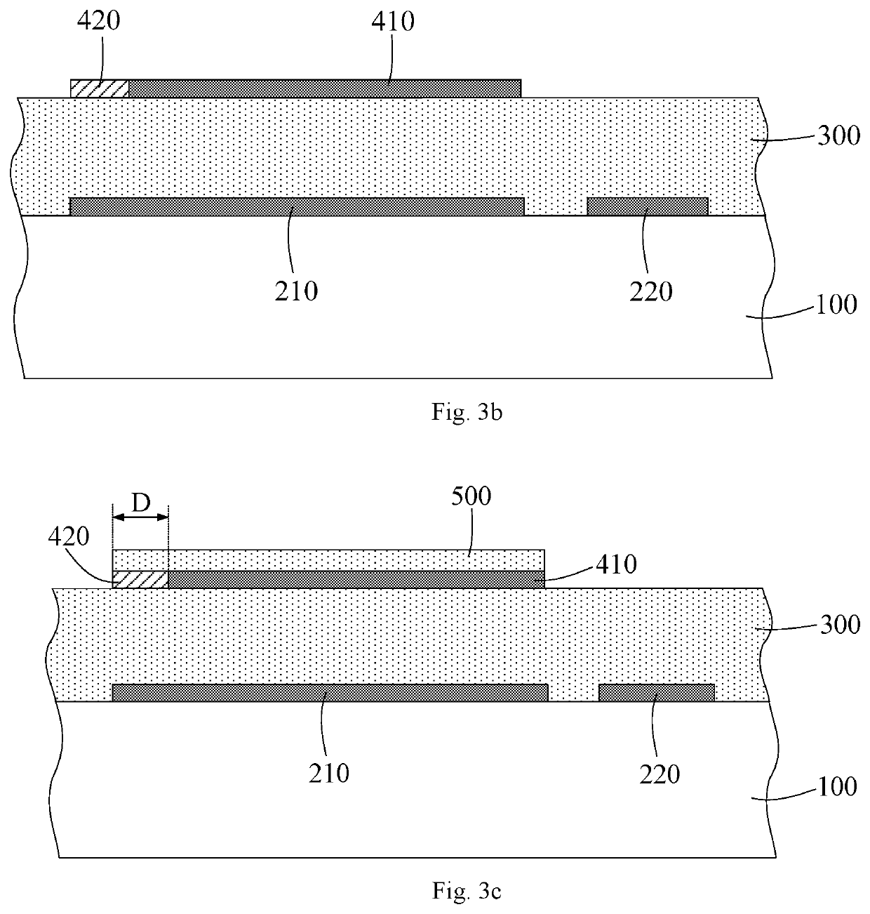
[0049]As described in the Background section, during the conventional semiconductor device fabrication, a suspended portion of a passivation layer is prone to damage in a subsequent process, which is harmful to the performance of the resulting semiconductor device. In order to overcome this problem, there is provided herein a method for fabricating a semiconductor device. For example, with reference to FIG. 2, the method includes:

[0050]in Step S100, providing a substrate having a lower electrode layer and a lead-out electrode formed thereon, the substrate further having a piezoelectric material layer formed over the lower electrode layer and the lead-out electrode;

[0051]in Step S200, forming an upper electrode layer and a sacrificial portion on the piezoelectric material layer, the sacrificial portion having a side surface adjacent to a side surface of the upper electrode layer at a first end thereof;

[0052]in Step S300, forming a passivation layer, which covers top surfaces of the u...


PUM

PropertyMeasurementUnit
widthaaaaaaaaaa
conductiveaaaaaaaaaa
converse piezoelectric effectaaaaaaaaaa

Abstract

A method of fabricating the semiconductor device includes the following steps. Forming a sacrificial portion at a first end of an upper electrode layer before a passivation layer is formed so that it supports a corresponding end portion of the passivation layer, making the passivation layer not suspended at all. In this way, the suspended portion of the passivation layer will not be damaged during the formation of a contact pad. In addition, subsequent to the formation of the contact pad, removing the sacrificial portion, freeing up a space under the end portion of the passivation layer so that the end portion itself becomes a suspended portion. This can ensure performance of the resulting semiconductor device.

Description

CROSS-REFERENCE TO RELATED APPLICATION[0001]This application claims the priority of Chinese patent application number 202010246888.2, filed on Mar. 31, 2020, the entire contents of which are incorporated herein by reference.TECHNICAL FIELD[0002]The present invention relates to the field of semiconductor technology and, in particular, to a semiconductor device and a method of fabricating the semiconductor device.BACKGROUND[0003]Semiconductor devices made of piezoelectric materials exhibiting the converse piezoelectric effect are key components of crystal oscillators and filters and are frequently used in bulk acoustic wave (BAW) filters. FIGS. 1a to 1b schematically show structures resulting from steps in a conventional method for fabricating a semiconductor device. As shown in FIGS. 1a and 1b, the method includes the steps detailed below.[0004]In Step 1, with particular reference to FIG. 1a, a substrate 10 is provided, on which a lower electrode layer 21 and a piezoelectric material...

Claims


Application Information

Patent Timeline
Patent Type & Authority Patents(United States)
IPC IPC(8): H04R17/00H01L41/083H01L41/297H01L41/09H01L41/332H01L41/047H03H9/54H01L41/293H01L41/27
CPCH01L41/0472H01L41/083H01L41/27H01L41/297H01L41/332H03H9/545H01L41/0471H01L41/09H01L41/293G03F7/42H10N30/87H10N30/88H10N30/02H10N30/06H03H9/171H03H9/02118H03H9/02125H03H3/02H10N30/063H10N30/05H10N30/20H10N30/50H10N30/067H10N30/082H10N30/871H10N30/872
Inventor WANG, YONGTAOWANG, CHONGCAI, MINHAOXIANG, SHAOHUA
Owner SEMICON MFG ELECTRONICS (SHAOXING) CORP
Why Eureka
Try Eureka