Organic electroluminescent device and display panel

a technology of electroluminescent devices and display panels, applied in semiconductor devices, solid-state devices, diodes, etc., can solve problems such as the increase of vacuum evaporation process defects

Active Publication Date: 2021-03-02
WUHAN CHINA STAR OPTOELECTRONICS SEMICON
View PDF16 Cites 1 Cited by
  • Summary
  • Abstract
  • Description
  • Claims
  • Application Information

AI Technical Summary

Benefits of technology

[0005]An embodiment of the present invention provides an organic electroluminescent device and a display panel to solve the problem of high defect rate of the existing organic electroluminescent device.
[0023]Beneficial effect of the present invention is that a first electron blocking layer and a first light-emitting layer are sequentially disposed in a first pixel region of an organic functional layer, and a first electron blocking layer, a first light-emitting layer, a second electron blocking layer, and a second light-emitting layer are sequentially disposed in the second pixel region of the organic functional layer, and the a first electron blocking layer, a first light-emitting layer, a second electron blocking layer, a second light-emitting layer, an electron blocking layer, and a third light-emitting layer are sequentially disposed in the third pixel region of the organic functional layer, wherein each of the second electron blocking layer and the third electron blocking layer in the second pixel region and the third pixel region is an integrally formed structure which is formed by using a semi-fine metal mask, to increase structural areas of the second electron blocking layer and the second light-emitting layer, thereby avoiding the use of a fine metal mask during preparation, thus reducing the defect rate of an organic electroluminescent device.

Problems solved by technology

Due to a high precision requirement, a complicated preparation process, and easy drooping of the fine metal mask, defects generated in the vacuum evaporation process increase with an increase in a number of uses of the high-definition metal mask.

Method used


Image

  • Organic electroluminescent device and display panel
  • Organic electroluminescent device and display panel
  • Organic electroluminescent device and display panel

Examples


Embodiment Construction

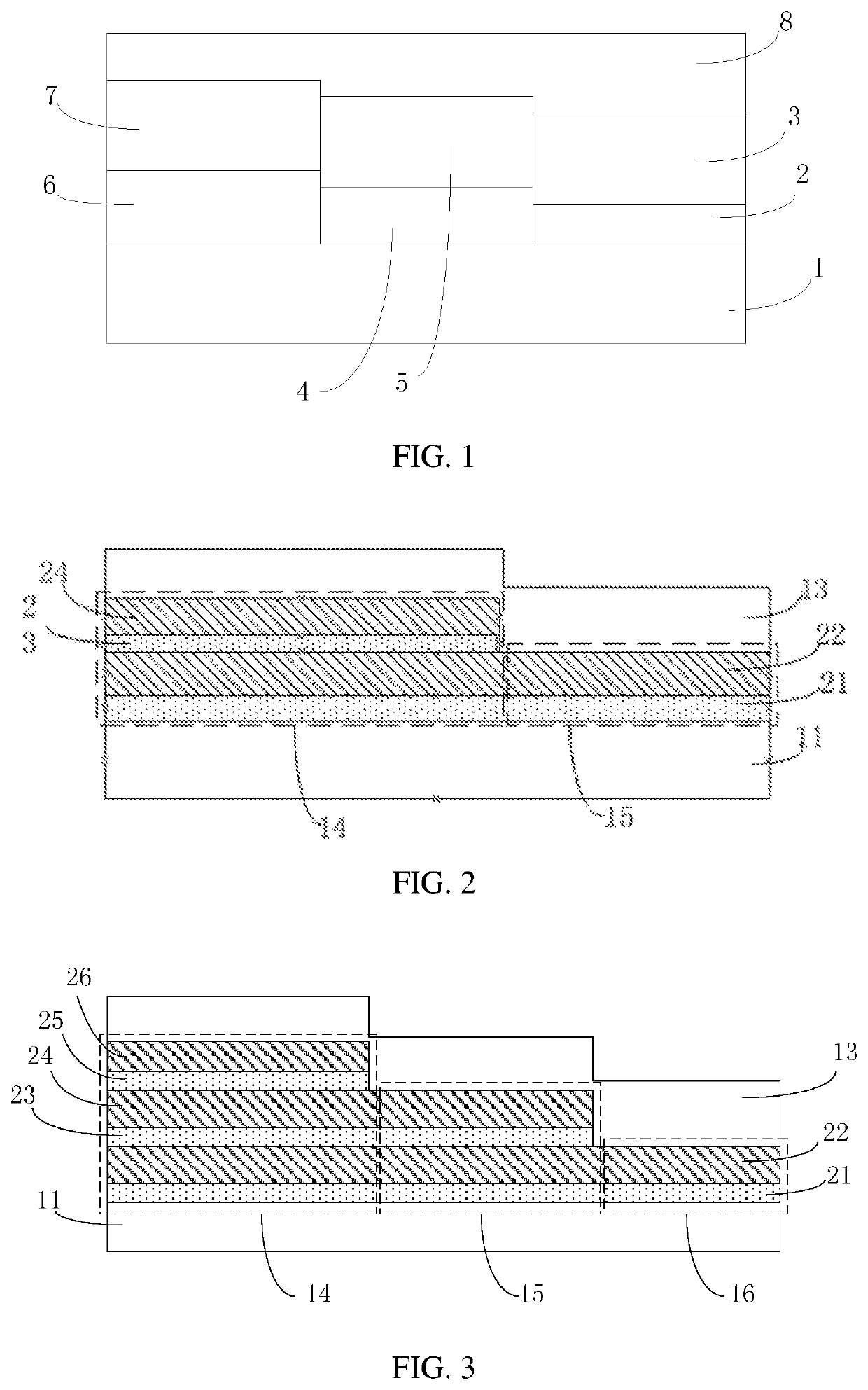
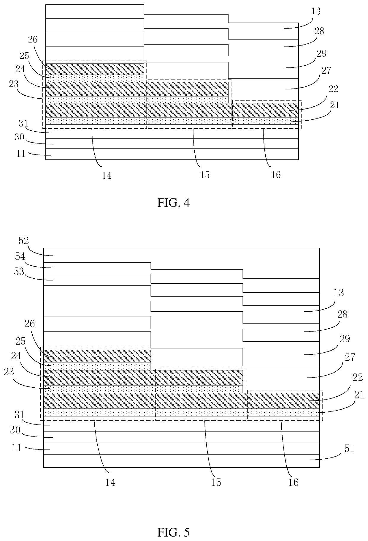
[0033]The preferred embodiments of the present invention are described below with reference to the accompanying drawings, which are used to exemplify the embodiments of the present invention, which can fully describe the technical contents of the present invention to make the technical content of the present invention clearer and easy to understand. However, the present invention may be embodied in many different forms of embodiments, and the scope of the present invention is not limited to the embodiments set forth herein.

[0034]The terms used in the description of the present invention are only used to describe specific embodiments, and it is not intended to show the concept of the invention. Expressions used in the singular encompasses the plural forms of expression unless the context clearly dictates otherwise. in the description of the present invention, it is to be understood that the terms such as “including”, “having” and “containing”, are intended to be illustrative of the p...


PUM

PropertyMeasurementUnit
organicaaaaaaaaaa
conductiveaaaaaaaaaa
colorsaaaaaaaaaa

Abstract

The invention discloses an organic electroluminescent device and a display panel. The organic electroluminescent device includes: a first electron blocking layer and a first light emitting layer in a first pixel region, a first electron blocking layer, a first light emitting layer, a second electron blocking layer, and a second light emitting layer in a second pixel region, and a first electron blocking layer, a first light emitting layer, a second electron blocking layer, a second light emitting layer, a third electron blocking layer, and a third light emitting layer in the third pixel region.

Description

BACKGROUND OF INVENTIONField of Invention[0001]The present invention relates to the field of display panel technologies, and in particular, to an organic electroluminescent device and a display panel.Description of Prior Art[0002]Organic electroluminescent diodes (OLEDs) are becoming a new generation of display devices that gradually replace liquid crystal displays (LCDs) because of their self-illumination, wide color gamut, fast response times, high contrast, low power consumption, and simple fabricating processes. In recent years, with the progressive application of organic electroluminescent diodes in televisions, mobile phones, and so on, the research and production of organic electroluminescent diodes has become a hot spot in the optoelectronic industry.[0003]The organic electroluminescent diode is formed by coating a thin film transistor (TFT) array substrate to form an organic material that can emit light independently, which is controlled by the TFT switch to achieve the pur...

Claims


Application Information

Patent Timeline
Patent Type & Authority Patents(United States)
IPC IPC(8): H01L51/50H01L27/32H01L51/52
CPCH01L51/5036H01L27/326H01L51/5056H01L51/5072H01L51/5096H01L51/5206H01L51/5221H10K59/32H10K59/35H10K71/166H10K50/13H10K50/18H10K50/125H10K50/15H10K50/16H10K50/81H10K50/82H10K59/121
Inventor YE, SHIQIAN
Owner WUHAN CHINA STAR OPTOELECTRONICS SEMICON
Why Eureka
Try Eureka