Substrate and display device including the same

a display device and substrate technology, applied in the direction of optics, instruments, printed circuit aspects, etc., can solve the problems of metal wiring cracks (e, generated) and achieve the effect of increasing the density of connection wirings

Active Publication Date: 2021-04-27
SAMSUNG DISPLAY CO LTD
View PDF9 Cites 0 Cited by
  • Summary
  • Abstract
  • Description
  • Claims
  • Application Information

AI Technical Summary

Benefits of technology

[0011]An aspect according to embodiments of the present disclosure may be directed to a display device capable of increasing a density of connection wirings.

Problems solved by technology

In this case, cracks may occur (e.g., may be generated) on a metal wiring located on the bent PCB.

Method used


Image

  • Substrate and display device including the same
  • Substrate and display device including the same
  • Substrate and display device including the same

Examples


Embodiment Construction

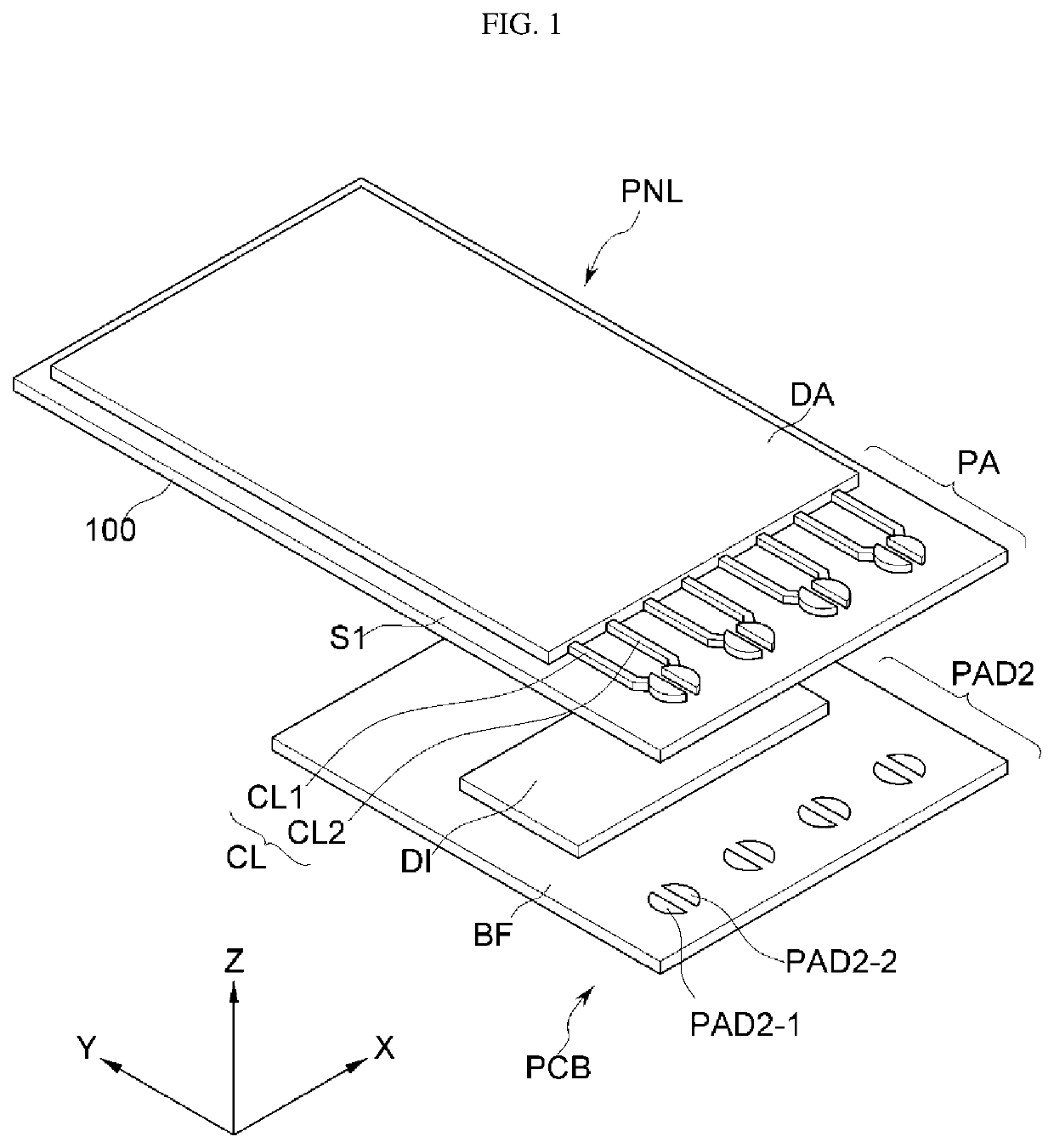
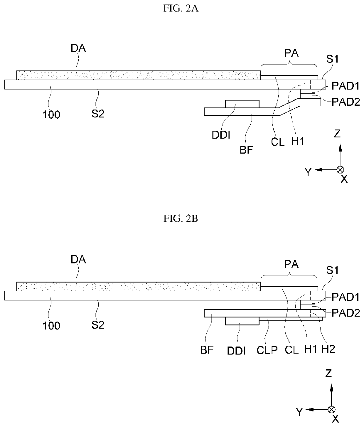
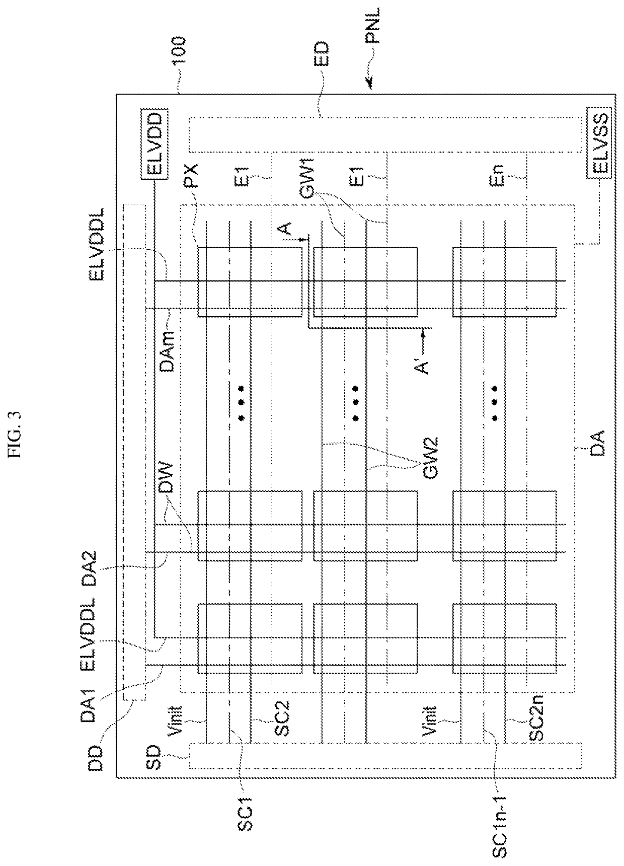
[0074]Embodiments will now be described more fully hereinafter with reference to the accompanying drawings. Although the invention may be modified in various suitable manners and have several embodiments, example embodiments are illustrated in the accompanying drawings and will be mainly described in the specification. However, the scope of the present invention is not limited to the embodiments and should be construed as including all the changes, equivalents and substitutions included in the spirit and scope of the present invention.

[0075]In the drawings, thicknesses of a plurality of layers and areas are illustrated in an enlarged manner for clarity and ease of description thereof. When a layer, area, or plate is referred to as being “on” another layer, area, or plate, it may be directly on the other layer, area, or plate, or intervening layers, areas, or plates may be present therebetween. Conversely, when a layer, area, or plate is referred to as being “directly on” another lay...


PUM

PropertyMeasurementUnit
diameteraaaaaaaaaa
thicknessaaaaaaaaaa
areaaaaaaaaaaa

Abstract

A display device includes: a substrate having a first surface, a second surface opposite to the first surface, and an inner side surface defining through holes; a first wiring and a second wiring disposed on the first surface; and a first conductor and a second conductor disposed in one of the through holes. The first conductor is connected to the first wiring, the second conductor is connected to the second wiring, and the first and second conductors are insulated from each other.

Description

CROSS-REFERENCE TO RELATED APPLICATION[0001]This application claims priority to and the benefit of Korean Patent Application No. 10-2018-0142903, filed on Nov. 19, 2018, in the Korean Intellectual Property Office (KIPO), the disclosure of which is incorporated by reference herein in its entirety.BACKGROUND1. Field[0002]Embodiments relate to a substrate and a display device including the substrate.2. Discussion of Related Art[0003]Display devices such as liquid crystal display (LCD) devices, plasma display devices (PDP), electrophoretic display devices, organic light emitting diode (OLED) display devices, field emission display (FED) devices, and electrophoretic display devices are currently being utilized.[0004]For example, an OLED display device includes two electrodes and an organic light emitting layer disposed between the two electrodes. Electrons injected from one electrode and holes injected from the other electrode are combined in the organic light emitting layer to form exci...

Claims


Application Information

Patent Timeline
Patent Type & Authority Patents(United States)
IPC IPC(8): H01L27/32
CPCH01L27/3276H01L27/3258H05K1/0296H10K59/131H05K2201/10128H05K1/141H05K1/115H05K2201/041H05K2201/09827H05K2201/09854G02F1/13452Y02E10/549H10K59/124H10K59/00H10K77/111
Inventor KIM, YOUNGSUKIM, DAWOONPARK, CHEULJINJUNG, SUKWON
Owner SAMSUNG DISPLAY CO LTD
Why Eureka
Try Eureka