Electrical contact material, method of producing an electrical contact material, and terminal

a technology of electrical contact material and terminal, which is applied in the direction of metal/alloy conductors, conductors, and conductors, can solve the problems of increasing the contact resistance at the outermost layer, and achieve the effect of suppressing the diffusion of material and suppressing the increase of contact resistan

Active Publication Date: 2021-05-04
FURUKAWA ELECTRIC CO LTD +1
View PDF17 Cites 0 Cited by
  • Summary
  • Abstract
  • Description
  • Claims
  • Application Information

AI Technical Summary

Benefits of technology

[0026]The electrical contact material of the present invention can suppress diffusion of the material of the conductive substrate into the outermost layer even in a high-temperature use environment, and can suppress the increase in contact resistance.

Problems solved by technology

Particularly, regarding the cause that controls the reliability of contact characteristics, there is a problem that under high-temperature conditions, the contact resistance at the outermost layer is increased as a result of diffusion of conductive substrate components and surface oxidation.

Method used


Image

  • Electrical contact material, method of producing an electrical contact material, and terminal

Examples


examples

[0057]The present invention will be described in more detail based on examples given below, but the invention is not meant to be limited by these.

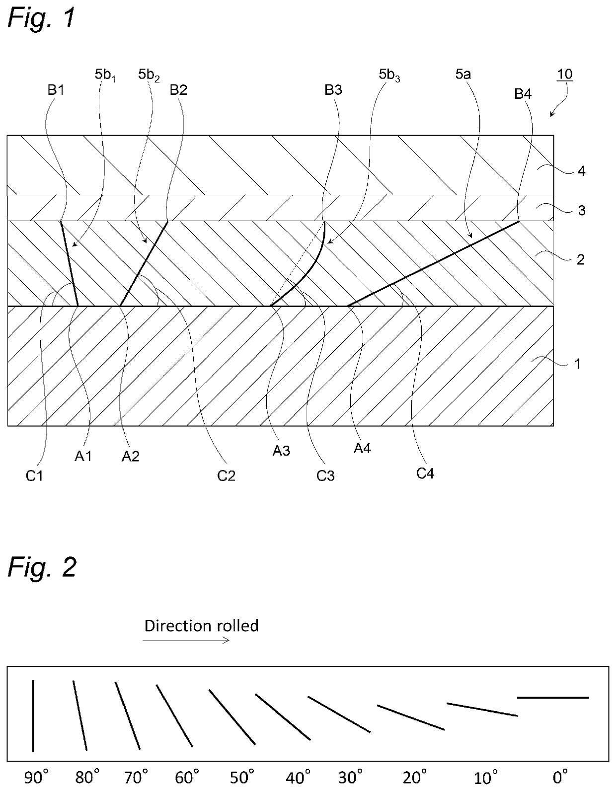
[0058]Each of the conductive substrates indicated in Table 1, having a thickness of 0.25 mm and a width of 50 mm, was subjected to preliminary treatments as described below (electrolytic degreasing and acid washing steps). Then, a Ni first intermediate layer, a Cu second intermediate layer, and a Sn outermost layer as indicated in Table 1 were provided under the conditions described below, and thereby the electrical contact materials of Examples and Comparative Examples indicated in Table 1 were obtained.

[0059]In Table 1, FAS680 and 7 / 3 bronze are as described above. MSP1 is C18665 (Cu—Mg—P-based alloy material, manufactured by Mitsubishi Shindoh Co., Ltd., trade name: MSP1).

[0060]Meanwhile, in an example in which a rolling was performed, after the Ni first intermediate layer was formed, or after the Cu second intermediate layer was formed...


PUM

PropertyMeasurementUnit
current densityaaaaaaaaaa
temperatureaaaaaaaaaa

Abstract

An electrical contact material (10) having: a conductive substrate (1) formed from copper or a copper alloy; a first intermediate layer (2) provided on the conductive substrate (1); a second intermediate layer (3) provided on the first intermediate layer (2); and an outermost layer (4) formed from tin or a tin alloy and provided on the second intermediate layer (3), wherein the first intermediate layer (2) is constructed as one layer of grains extending from the conductive substrate (1) side to the second intermediate layer (3) side, and wherein, in the first intermediate layer (2), the density of grain boundaries (5b) extending in a direction in which the angle formed by the grain boundary in interest and the interface between the conductive substrate and the first intermediate layer is 45° or greater, is 4 μm / μm2 or less; a method of producing the same; and a terminal.

Description

CROSS-REFERENCE TO RELATED APPLICATIONS[0001]This application is a Continuation of PCT International Application No. PCT / JP2015 / 065819 filed on Jun. 1, 2015, which claims priority under 35 U.S.C. § 119 (a) to Japanese Patent Application No. 2014-112973 filed in Japan on May 30, 2014. Each of the above applications is hereby expressly incorporated by reference, in its entirety, into the present application.TECHNICAL FIELD[0002]The present invention relates to an electrical contact material, a method of producing an electrical contact material, and a terminal.BACKGROUND ART[0003]Hitherto, in electrical contact materials, copper or a copper alloy having excellent electrical conductivity has been utilized; however, in recent years, enhancement of contact characteristics have progressed, and the number of cases in which copper or a copper alloy is directly used is decreasing. Instead of such a conventional material, materials obtained by subjecting copper or a copper alloy to any of vari...

Claims


Application Information

Patent Timeline
Patent Type & Authority Patents(United States)
IPC IPC(8): H01B1/02C25D5/12H01H1/025B21D53/00H01H1/04C25D5/50B32B15/01C22F1/10C25D5/34C25D7/00C22F1/08C22F1/16C25D3/12C25D3/30C25D3/38
CPCH01B1/026B21D53/00B32B15/01B32B15/018C22F1/08C22F1/10C22F1/16C25D5/12C25D5/50C25D5/505C25D7/00H01H1/025H01H1/04C25D3/12C25D3/30C25D3/38C25D5/34Y10T428/1291Y10T428/12715
Inventor OKUNO, YOSHIKAZUKOBAYASHI, YOSHIAKINAKATSUGAWA, TATSUYAMITOSE, KENGOTACHIBANA, AKIRAKAWATA, SHINGO
Owner FURUKAWA ELECTRIC CO LTD
Why Eureka
Try Eureka