Method of producing laminated substrate, method of producing semiconductor module, laminated substrate, and semiconductor module

a technology of laminated substrates and semiconductor modules, applied in the direction of semiconductor devices, solid-state devices, basic electric elements, etc., can solve the problems of insufficient dielectric breakdown voltage, many defects, and pits around the edge of electrodes, and achieve high-reliable semiconductor modules and stable production. , the effect of high dielectric breakdown voltag

Active Publication Date: 2021-05-11
FUJI ELECTRIC CO LTD
View PDF7 Cites 0 Cited by
  • Summary
  • Abstract
  • Description
  • Claims
  • Application Information

AI Technical Summary

Benefits of technology

[0007]Incidentally, electric fields concentrate around an edge of an electrode. This often causes dielectric breakdown. Patent Documents 1 and 2 for example disclose a technique in which a solid insulator fills the space between an edge of an electrode and a surface of a ceramic substrate. This configuration is believed to increase the dielectric breakdown voltage.
[0012]In view of this problem, it is an object of the present disclosure to provide a method of producing a laminated substrate and a laminated substrate that can achieve a higher dielectric breakdown voltage easily and stably and to provide a method of producing a semiconductor module and a semiconductor module that can achieve higher reliability.
[0015]The method of producing a laminated substrate according to the present disclosure realizes stable production of a laminated substrate having a high dielectric breakdown voltage through a simple scheme. This permits production of highly-reliable semiconductor modules.
[0016]The laminated substrate according to the present disclosure can achieve a higher dielectric breakdown voltage in a stable manner. Thereby, highly-reliable semiconductor modules can be provided.

Problems solved by technology

This often causes dielectric breakdown.
However, many defects, known as pits, emerge around an edge of an electrode.
This prevents the solid insulator from appropriately filling the defects, resulting in an insufficient dielectric breakdown voltage.
However, the etching for forming the electrode has caused a defect on the surface of the externally extending portion of the junction layer.
This prevents the coating material from appropriately filling the defect in the junction layer, resulting in an insufficient dielectric breakdown voltage.
Further, the solid insulators and the coating materials appearing in the above Patent Documents may peel off.
These approaches based on the above Patent Documents fail to provide sufficient reliability for semiconductor modules that are produced by using laminated substrates described in these Patent Documents.

Method used


Image

  • Method of producing laminated substrate, method of producing semiconductor module, laminated substrate, and semiconductor module
  • Method of producing laminated substrate, method of producing semiconductor module, laminated substrate, and semiconductor module
  • Method of producing laminated substrate, method of producing semiconductor module, laminated substrate, and semiconductor module

Examples


Embodiment Construction

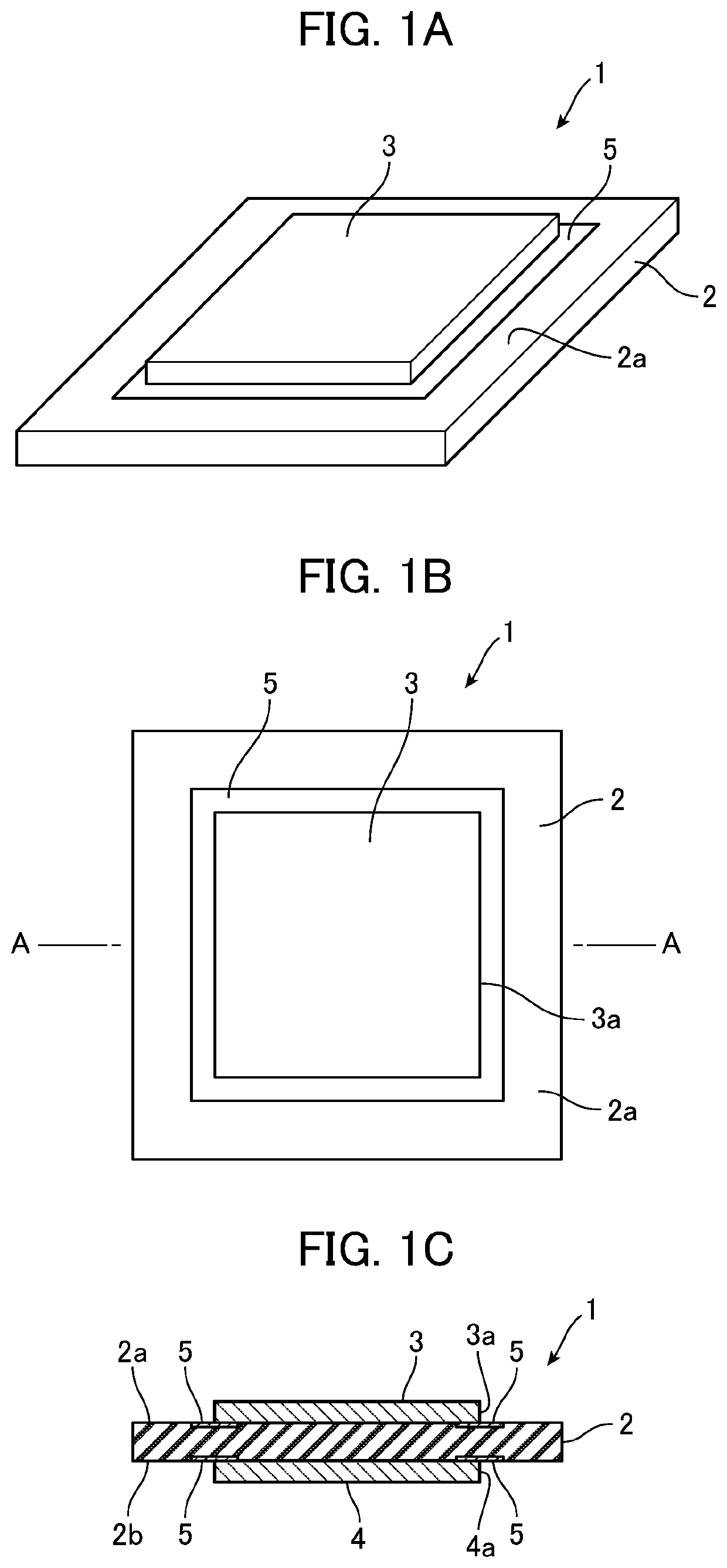
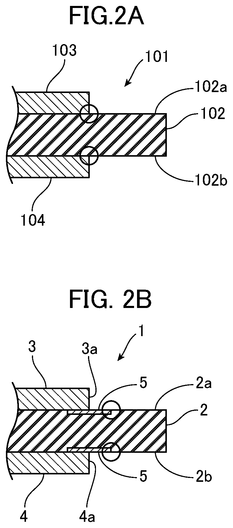
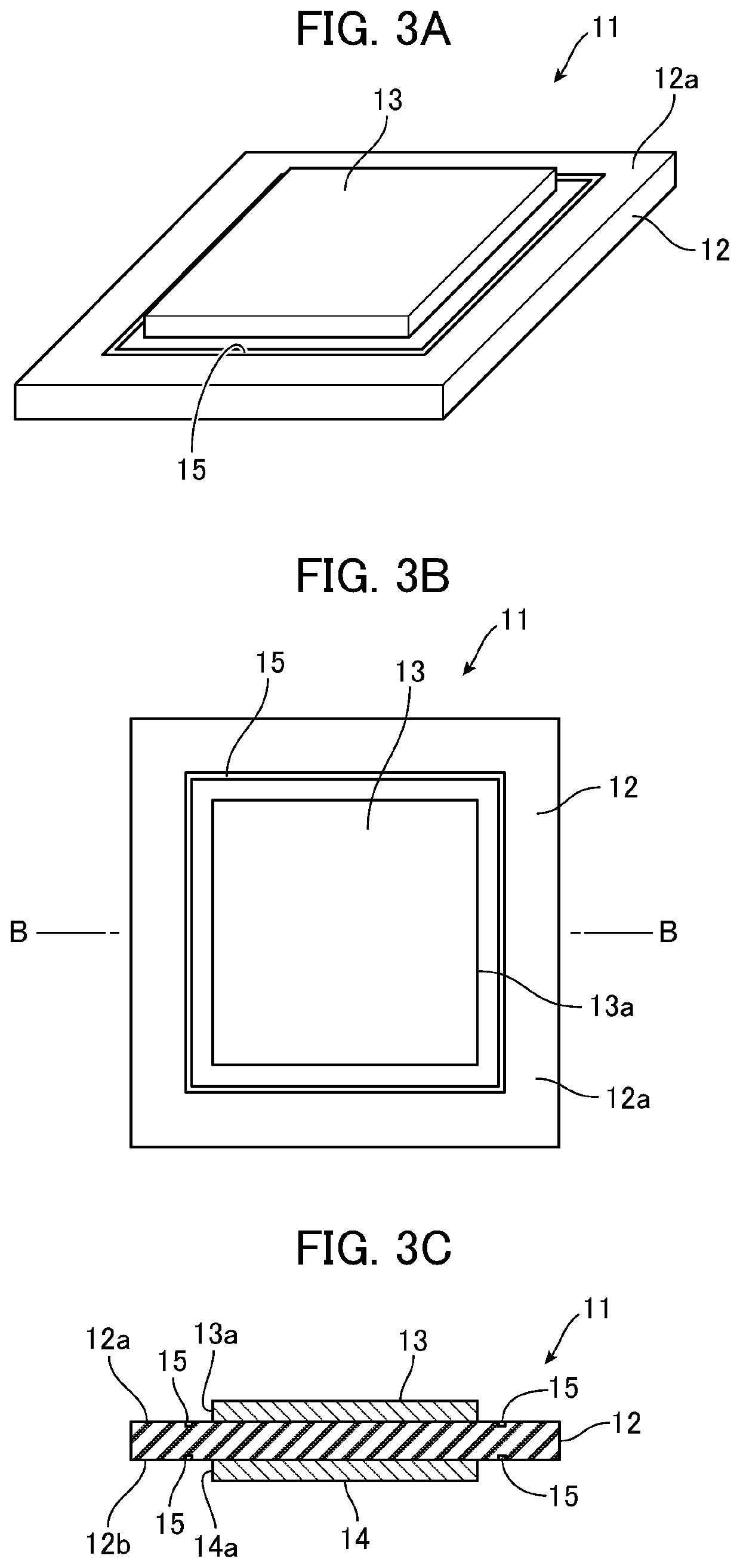
[0041]The following will explain a laminated substrate of a first embodiment. FIG. 1A is a perspective view of the laminated substrate of the first embodiment. FIG. 1B is a plan view of the same laminated substrate. FIG. 1C is a cut-portion end view of the same laminated substrate. The cut-portion end view of FIG. 1C illustrates the end surface resulting from cutting the laminated substrate along line A-A of FIG. 1B. FIG. 1A through FIG. 1C will be referred to for explaining the components constituting the laminated substrate as well as a method of producing the laminated substrate, particularly, laser processing applied to the insulation substrate.

[0042]As illustrated in FIG. 1A through FIG. 1C, a laminated substrate 1 includes an insulation substrate 2 comprising ceramic, and electrodes 3 and 4 formed respectively on top surface (front surface) 2a and bottom surface (rear surface) 2b of the insulation substrate 2. The electrodes 3 and 4 respectively have areas smaller than those o...


PUM

PropertyMeasurementUnit
conductive propertyaaaaaaaaaa
electrical conductivityaaaaaaaaaa
metallicaaaaaaaaaa

Abstract

A method of manufacturing a laminated substrate including an insulation substrate comprised of ceramic, and a front electrode formed on a front surface of the insulation substrate, a semiconductor element being mountable on a front surface of the front electrode, including forming the front electrode on the front surface of the insulation substrate, and before or after the forming the front electrode, applying laser processing to the front surface of the insulation substrate at an outer peripheral area of the front electrode to modify a conductive property of the front surface of the insulation substrate to have electrical conductivity.

Description

CROSS REFERENCE TO RELATED APPLICATION[0001]This application is based upon and claims the benefit of priority from the prior Japanese Patent Application No. 2018-146412, filed on Aug. 3, 2018; the entire contents of which are incorporated herein by reference.FIELD OF THE INVENTION[0002]The present disclosure is related to a method of producing a laminated substrate, a method of producing a semiconductor module, a laminated substrate, and a semiconductor module.DESCRIPTION OF THE RELATED ART[0003]A laminated substrate fora semiconductor module includes a ceramic substrate such as for example a substrate containing aluminum nitride (AlN), and an electrode provided on a surface of the ceramic substrate (see Patent Documents 1 through 3). A semiconductor element is mounted on a surface of the electrode.PRIOR ART DOCUMENTSPatent Documents[0004][Patent Document 1] Japanese Laid-open Patent Publication No. 2002-76197[0005][Patent Document 2] Japanese Laid-open Patent Publication No. 2002-7...

Claims


Application Information

Patent Timeline
Patent Type & Authority Patents(United States)
IPC IPC(8): H01L23/62H01L21/48H01L23/373H01L23/043H01L25/07H01L23/00
CPCH01L23/62H01L21/4882H01L23/043H01L23/3735H01L24/32H01L25/072H01L2224/32225H01L2924/10253H01L2924/10272H01L2924/12032H01L2924/13055H01L2924/13091H01L23/13H01L23/14H01L23/053H01L23/49838H01L23/5386H01L25/18H01L25/50C04B37/021C04B37/026C04B2237/366H01L24/29H01L2224/32227H01L21/4846H01L2224/291H01L2924/014
Inventor YAMASHIRO, KEISUKE
Owner FUJI ELECTRIC CO LTD
Why Eureka
Try Eureka