Semiconductor device

A technology of semiconductors and field effect transistors, applied in the field of semiconductor devices, can solve the problems of monolithic microwave integrated circuits, low thermal conductivity, difficult temperature management and atmospheric gas management, etc.

Inactive Publication Date: 2003-12-17
PANASONIC CORP
View PDF0 Cites 0 Cited by
  • Summary
  • Abstract
  • Description
  • Claims
  • Application Information

AI Technical Summary

Problems solved by technology

[0008] However, in order to form the ohmic electrode 102A in the method for forming the ohmic electrode in the first existing embodiment, the substrate 101 made of silicon carbide is subjected to a high-temperature treatment close to the temperature at which silicon carbide crystals are formed, and damage to the substrate 101 must be avoided. Damage, high-frequency heating furnace 103 for high-temperature heat treatment requires special equipment, temperature management and atmosphere gas management to set optimal conditions are very difficult in the high-temperature heat treatment process, and complex operation management such as high-temperature safety management is required various problems
[0009] In addition, since the monolithic microwave integrated circuit (MMIC) of the second conventional embodiment has a lower thermal conductivity of 0.5 W / cm·K than gallium arsenide used for the substrate 111, if it is desired to increase the output of the high-output amplifier 112 , the temperature of the substrate 111 will rise. Due to the problem of high electron mobility (about 6000 cm·cm / Vs) of gallium arsenide, the noise characteristics of the low noise amplifier 113 will deteriorate. As a result, the output will be from several watts to several A monolithic microwave integrated circuit of a high output amplifier of one hundred watts is difficult

Method used


Image

  • Semiconductor device
  • Semiconductor device
  • Semiconductor device

Examples


no. 1 example

[0046] Next, a first embodiment of the present invention will be described with reference to the drawings.

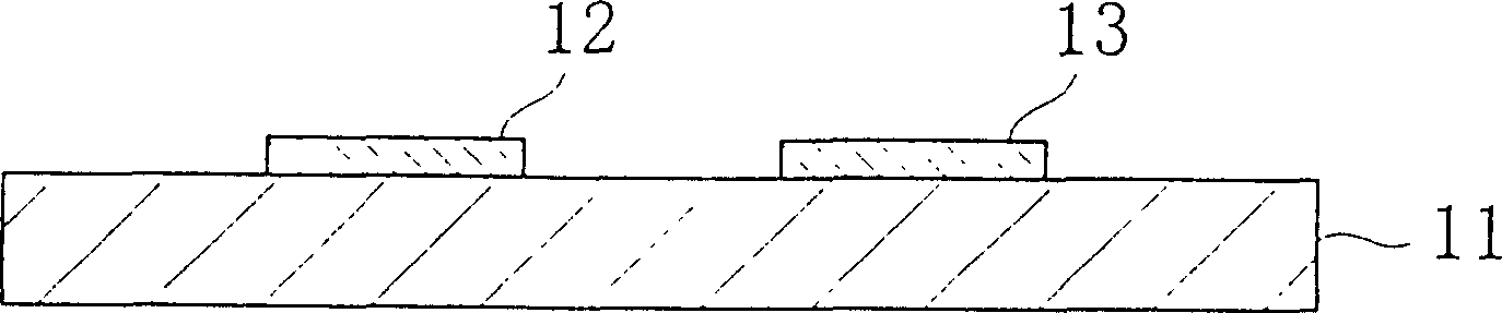
[0047] 1( a ) to ( c ) are cross-sectional structural views showing the procedure of the method for forming an ohmic electrode according to the first embodiment of the present invention. First, as shown in FIG. 1( a ), a first metal film 12 and a second metal film 13 made of nickel (Ni) or the like are deposited on a substrate 11 made of silicon carbide, for example, by vapor deposition. In this state, the interface between the first metal film 12 and the substrate 11 and the interface between the second metal film 13 and the substrate 11 are not in ohmic contact, but are Schottky contacts in common.

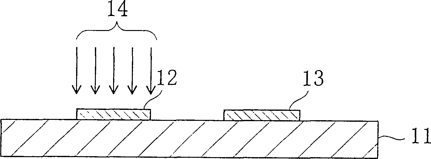
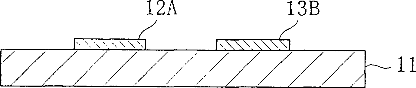
[0048] Next, as shown in FIG. 1( b ), only the first metal film 12 of the substrate 11 is irradiated with the laser light 14 whose tip is narrowed from the upper surface of the substrate 11 . Therefore, as shown in FIG. 1( c), even if the substrate 11 is not heated, the ...

no. 2 example

[0054] Next, a second embodiment of the present invention will be described with reference to the drawings.

[0055] 2( a ) to ( c ) are cross-sectional structural diagrams showing the procedure of the ohmic electrode forming method according to the second embodiment of the present invention. First, as shown in FIG. 2( a ), a first metal film 22 and a second metal film 23 made of nickel or the like are deposited on a substrate 21 made of silicon carbide using a vapor deposition method. In this state, the first metal film 22 and the second metal film 23 are in Schottky contact with the substrate 21, respectively. Afterwards, using an electroplating method, a first electroplated metal film 24 is deposited on the first metal film 22 , and a second electroplated metal film 25 is deposited on the second metal film 23 .

[0056] Next, as shown in FIG. 2( b ), from the upper surface of the substrate 21 , only the first metal plating film 24 in the substrate 21 is irradiated with the...

no. 3 example

[0061] Next, a third embodiment of the present invention will be described with reference to the drawings.

[0062] 3( a ) to ( c ) are cross-sectional structural diagrams showing the procedure of the method for forming an ohmic electrode according to the third embodiment of the present invention. First, as shown in FIG. 3( a ), a first metal film 32 and a second metal film 33 made of nickel or the like are deposited on the surface of a substrate 31 made of silicon carbide. In this state, each interface between the first metal film 32 and the second metal film 33 and the substrate 11 is a Schottky contact in common.

[0063]Next, as shown in FIG. 3( b), the wavelength of irradiation of the substrate 31 from the surface side of the substrate 31 is a wavelength corresponding to the energy corresponding to the forbidden band (=Eg) of silicon carbide (=h·c / Eg) compared with laser light 34 having a sufficiently long wavelength. Thus, as shown in FIG. 3( c), even if the substrate...


PUM


Abstract

A first metal film and a second metal film, both of which are made of Ni or the like, are deposited on the upper surface of a substrate made of SiC. In such a state, the interface between the first metal film and the substrate and the interface between the second metal film and the substrate both form a Schottky contact. Next, laser light is irradiated from above the upper surface of the substrate only onto the first metal film on the substrate after the diameter of the top end of the laser light has been reduced. Thus, since the metal-semiconductor interface between the first metal film and the substrate is turned into an alloy owing to the energy of the laser light without heating the entire substrate, an ohmic contact can be formed in the interface between the first metal film and the substrate. As a result, an ohmic electrode can be constituted by the first metal film.

Description

technical field [0001] The present invention relates to an ohmic electrode forming method for forming an ohmic electrode on a substrate formed of silicon carbide having a large band gap, and a transmission amplifier requiring high output characteristics and a transmission amplifier requiring low noise characteristics using the substrate formed of silicon carbide A semiconductor device in which a receiving amplifier is integrated. Background technique [0002] In recent years, silicon carbide (SiC) has attracted worldwide attention as a next-generation semiconductor material due to its superiority in wide bandgap characteristics and abundant constituent elements. Since the silicon carbide crystal structure is a covalent bond, the substance is extremely stable, and, due to the large band gap and high melting point, high temperature heat treatment is required to form an ohmic electrode on silicon carbide. [0003] Next, a method of forming an ohmic electrode using a high-tempe...

Claims


Application Information

Patent Timeline
Patent Type & Authority Patents(China)
IPC IPC(8): H01L21/04H01L21/8258
CPCH01L29/66068H01L21/0485Y10S438/931H01L21/8258H01L21/0495H01L29/6606H01L21/268
Inventor 太田顺道正户宏幸熊渕康仁北畠真
Owner PANASONIC CORP
Why Eureka
Try Eureka