Semiconductor device

a technology of semiconductor elements and sealing materials, applied in semiconductor devices, semiconductor/solid-state device details, electrical devices, etc., can solve the problems of reducing the reliability of the semiconductor device, peeling the small area of adhesion between the sealing material and the insulating substrate, etc., to achieve the effect of increasing the packaging density of semiconductor elements, reducing size, and reducing siz

Active Publication Date: 2021-06-08
MITSUBISHI ELECTRIC CORP
View PDF9 Cites 0 Cited by
  • Summary
  • Abstract
  • Description
  • Claims
  • Application Information

AI Technical Summary

Benefits of technology

[0011]According to the semiconductor device, the case member is provided with the recess that is continuous with the connection portion between the case member and the insulating substrate and that has a sufficient size in the semiconductor device having an increased packaging density of semiconductor elements and reduced in size. Therefore, the recess can be reliably filled with the sealing material, to increase the area of joint between the sealing material and the insulating substrate as compared to an example where the recess is not provided. Thus, the joint strength between the sealing material and the insulating substrate can be improved to increase resistance to thermal stress in the semiconductor device reduced in size. As a result, the semiconductor device reduced in size and having high reliability can be obtained.

Problems solved by technology

As a result, the area of adhesion between a sealing material that protects the semiconductor elements and the insulating substrate tends to be small.
The small area of adhesion may cause peeling between the sealing material and the insulating substrate due to stress caused by high temperature storage or a heat cycle in the semiconductor device.
There is a risk that such peeling between the sealing material and the insulating substrate may reduce insulation of the semiconductor device, resulting in reduced reliability of the semiconductor device.

Method used


Image

  • Semiconductor device
  • Semiconductor device
  • Semiconductor device

Examples


first embodiment

[0027]

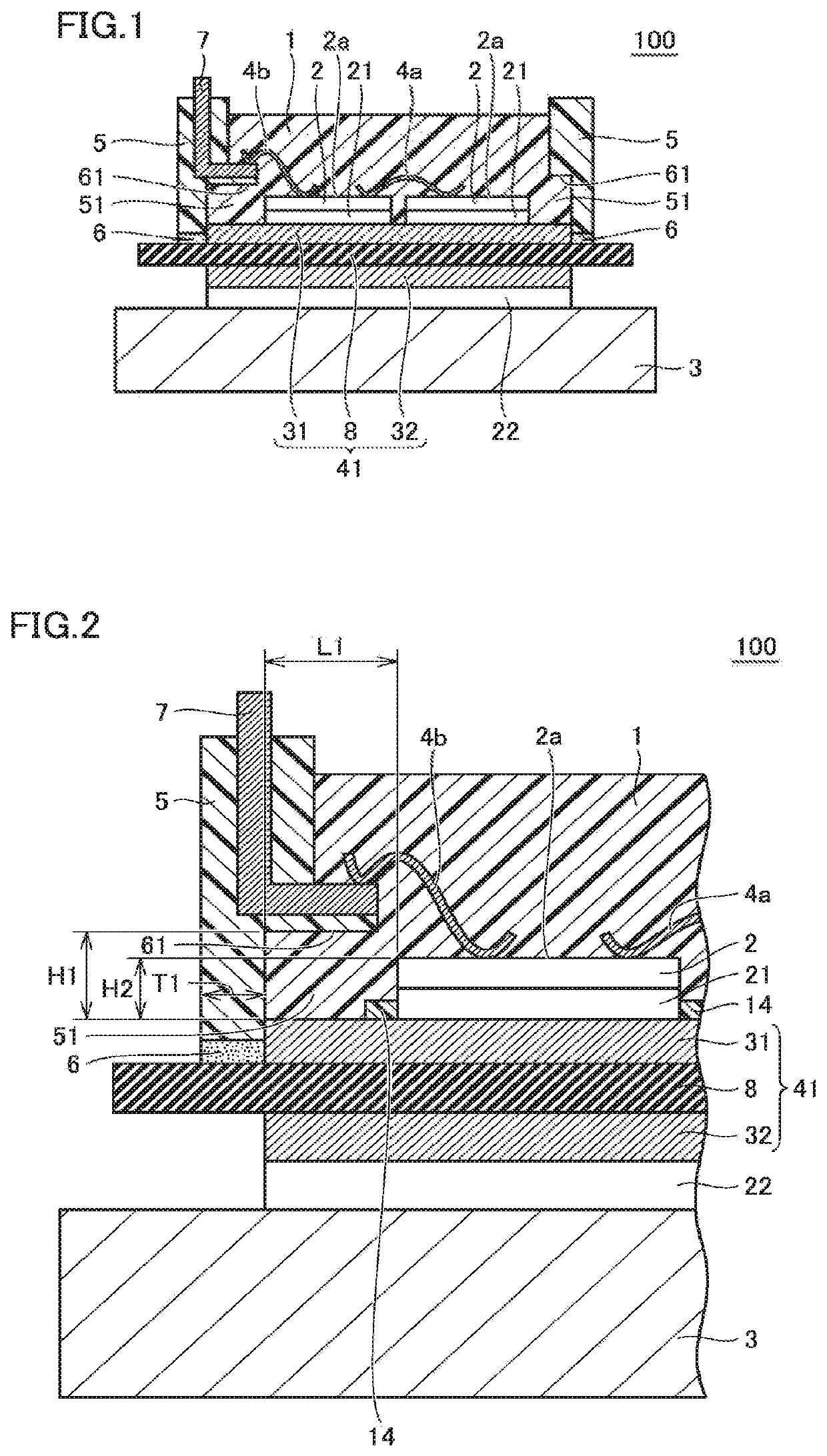
[0028]FIG. 1 is a schematic cross-sectional view showing a basic structure of a semiconductor device according to a first embodiment of the present invention. FIG. 2 is a schematic fragmentary cross-sectional view of the semiconductor device shown in FIG. 1. The configuration of the semiconductor device according to the first embodiment of the present invention is described with reference to FIGS. 1 and 2. A semiconductor device 100 shown in FIGS. 1 and 2 is a semiconductor power module used for industrial purposes or for automobiles, for example.

[0029]Referring to FIG. 1, semiconductor device 100 mainly includes an insulating substrate 41, a metal base plate 3, semiconductor elements 2 joined on insulating substrate 41, wiring members 4a, 4b, a case member 5 surrounding semiconductor elements 2, an electrode terminal 7, and a sealing resin 1. Case member 5 is connected to insulating substrate 41 by an adhesive 6. Case member 5 is provided with a recess 51 on its inner surface...

second embodiment

[0062]

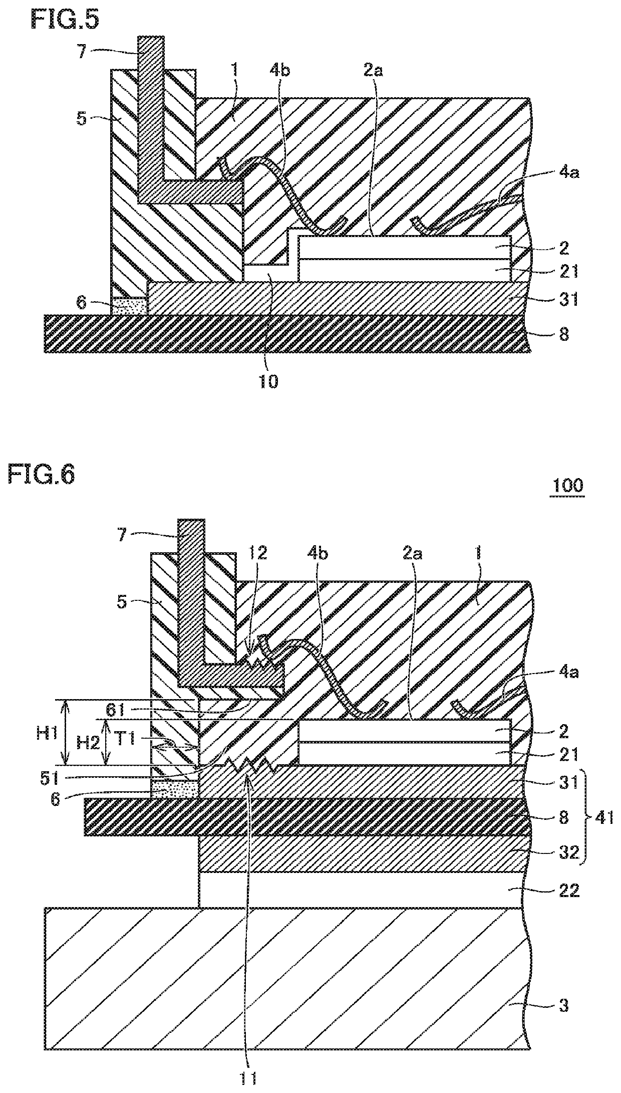
[0063]FIG. 8 is a schematic cross-sectional view showing a basic structure of a semiconductor device 200 according to a second embodiment of the present invention. The configuration of semiconductor device 200 according to the second embodiment of the present invention is described with reference to FIG. 8.

[0064]As shown in FIG. 8, semiconductor device 200 is basically configured similarly to the semiconductor device shown in FIGS. 1 and 2, but is different from semiconductor device 100 shown in FIGS. 1 and 2 in that it has a through hole 9 provided in case member 5. That is, semiconductor device 200 shown in FIG. 8 is provided with through hole 9 extending from inside recess 51 to an upper end of case member 5.

[0065]

[0066]Semiconductor device 200 shown in FIG. 8 can basically produce similar effects to those of semiconductor device 100 shown in FIG. 1. Further, in semiconductor device 200 shown in FIG. 8, through hole 9 provided in case member 5 extends through case member 5 ...

third embodiment

[0076]

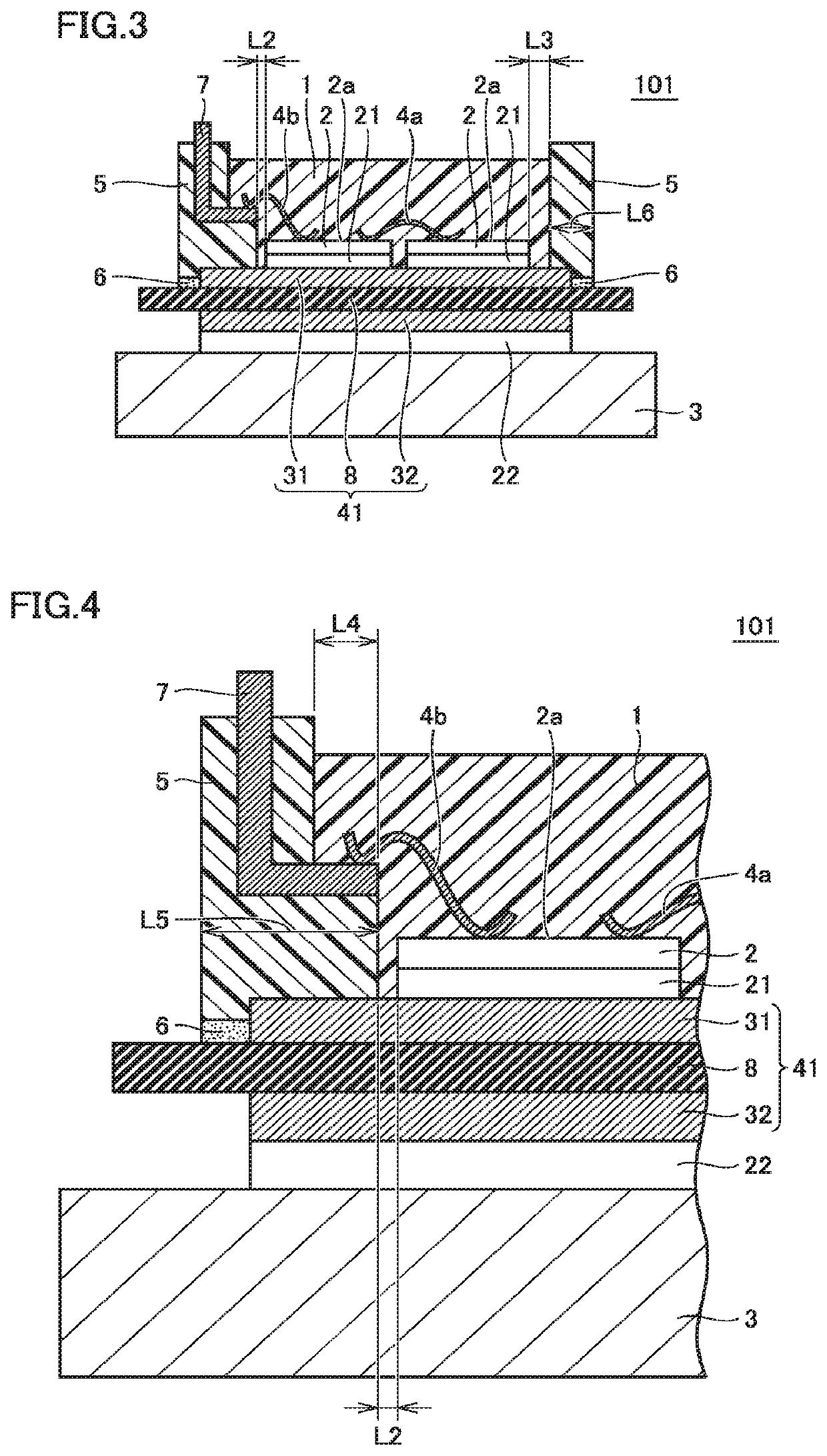
[0077]FIG. 12 is a schematic cross-sectional view showing a basic structure of a semiconductor device 300 according to a third embodiment of the present invention. The configuration of semiconductor device 300 according to the third embodiment of the present invention is described with reference to FIG. 12.

[0078]As shown in FIG. 12, semiconductor device 300 is basically configured similarly to semiconductor device 200 shown in FIG. 8, but is different from semiconductor device 200 shown in FIG. 8 in the shape of the inner wall of recess 51. That is, in semiconductor device 300 shown in FIG. 12, facing surface 61 of recess 51 facing insulating substrate 41 is inclined relative to the front surface of insulating layer 8 or the surface of first circuit board 31. In other words, facing surface 61 of recess 51 is a surface inclined such that its distance from insulating layer 8 or first circuit board 31 increases gradually from the end on the outer peripheral side to the end on the...


PUM

PropertyMeasurementUnit
Distance H1aaaaaaaaaa
distance H1aaaaaaaaaa

Abstract

A semiconductor device includes an insulating substrate having a main surface, a semiconductor element, a case member, and a sealing resin as a sealing material. The case member includes a recess that is continuous with a connection portion of the case member connected to the insulating substrate, and that faces the internal region. The recess includes a facing surface as an inner wall portion facing the main surface of the insulating substrate. A distance from the main surface of the insulating substrate to the facing surface as the inner wall portion is greater than a distance from the main surface to an upper surface of the semiconductor element.

Description

TECHNICAL FIELD[0001]The present invention relates to a semiconductor device in which a semiconductor element disposed on an insulating substrate is sealed with a sealing resin.BACKGROUND ART[0002]There is a need for semiconductor devices such as inverter devices mounted on industrial equipment and automobiles to have higher density and smaller size. This need has led to increasing packaging density of semiconductor elements packaged on those semiconductor devices. In a semiconductor device having a high packaging density of semiconductor elements, an exposed area of an insulating substrate on which the semiconductor elements are packaged is relatively small. As a result, the area of adhesion between a sealing material that protects the semiconductor elements and the insulating substrate tends to be small. The small area of adhesion may cause peeling between the sealing material and the insulating substrate due to stress caused by high temperature storage or a heat cycle in the semi...

Claims


Application Information

Patent Timeline
Patent Type & Authority Patents(United States)
IPC IPC(8): H01L23/053H01L23/373H01L25/07H01L23/00H01L23/29H01L23/31
CPCH01L23/562H01L23/053H01L23/293H01L23/296H01L23/3121H01L23/3735H01L24/48H01L24/73H01L25/072H01L2224/48137H01L2224/48155H01L2224/48472H01L2224/73265H01L2924/0665H01L2924/0715H01L2924/35121H01L2924/181H02M7/48H01L25/18H01L2224/32225H01L23/24H01L23/04H01L23/10H01L23/3142H01L21/54H01L23/36H01L2224/49175H01L2224/49111H01L2224/48091H01L2224/49109H01L2224/26165H01L2224/8314H01L24/83H01L2924/00014H01L24/49H01L2224/83007H01L24/32H01L2924/18301H01L2224/8592H01L24/85H01L2924/3641H01L2924/1715H01L2924/00012H01L2224/45099H01L2224/29099
Inventor KAJI, YUSUKEHARADA, KOZO
Owner MITSUBISHI ELECTRIC CORP
Why Eureka
Try Eureka