
Touch detection circuit, input device and electronic apparatus

a detection circuit and input device technology, applied in the direction of resistance/reactance/impedence, instruments, pulse techniques, etc., can solve the problems of not only inability to detect water drops attached to touch-style input devices, but also inability to detect two-point touch

Active Publication Date: 2021-07-06
ROHM CO LTD
View PDF4 Cites 0 Cited by
  • Summary
  • Abstract
  • Description
  • Claims
  • Application Information

AI Technical Summary

Benefits of technology

The solution effectively cancels parasitic capacitance, enabling high-sensitivity detection of electrostatic capacitance and supporting multi-point touch recognition while maintaining resistance to water interference.

Problems solved by technology

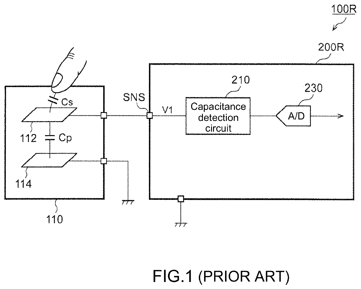
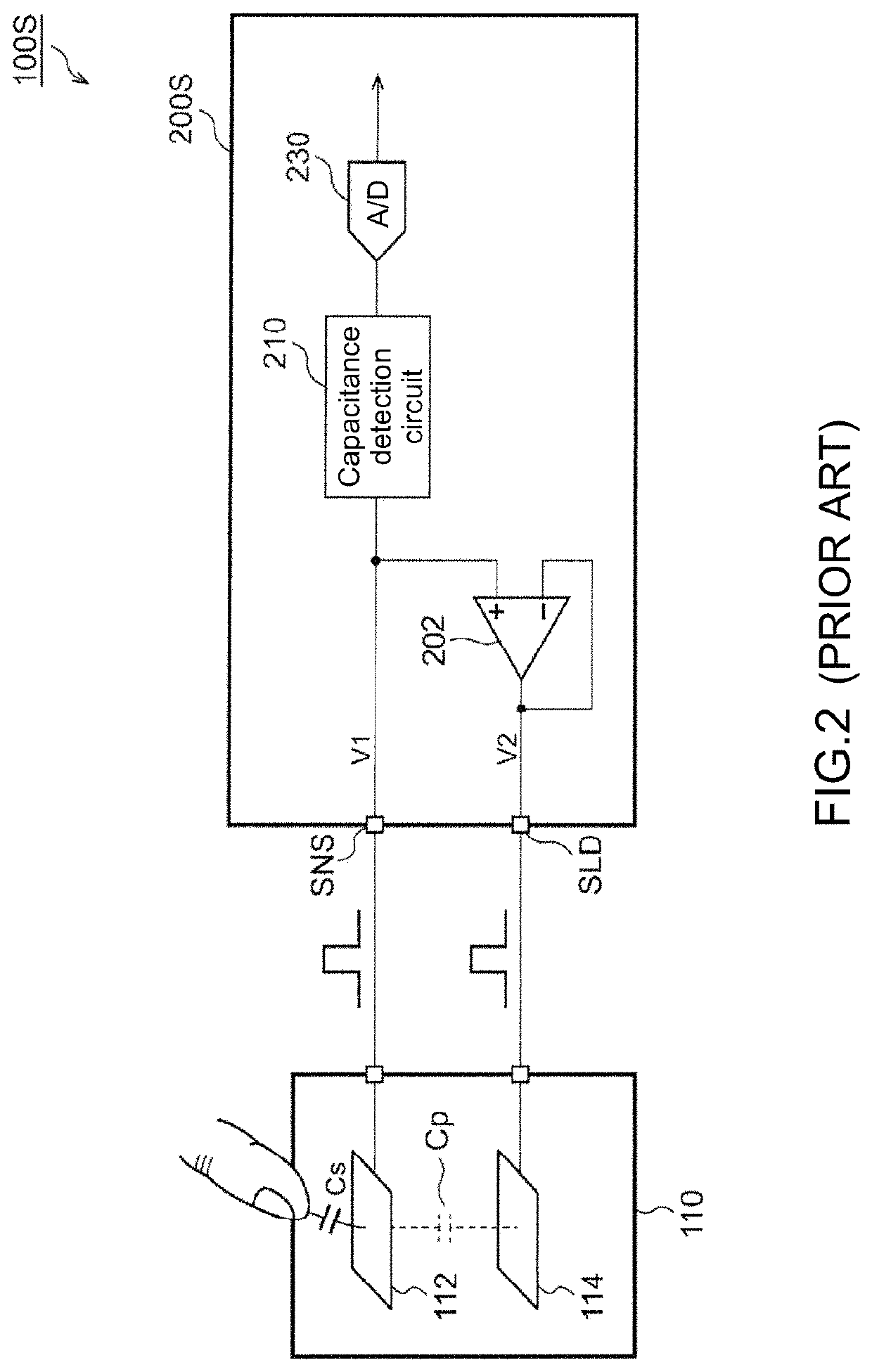
The self-capacitance type is highly sensitive, as it not only detects a touch but also detects the approach of a finger; however, it is not only unable to discern any water drops attached to the touch-style input devices but also fails to detect a two-point touch.

Method used


Image

  • Touch detection circuit, input device and electronic apparatus
  • Touch detection circuit, input device and electronic apparatus
  • Touch detection circuit, input device and electronic apparatus

Examples


embodiment 1

Variant Embodiment 1

[0099]FIG. 9 is an action waveform diagram of the touch detection circuit 200 in variant embodiment 1. In the variant embodiment, the simultaneously-on time period of the first switch SW11 and the second switch SW12 starts immediately after the transition from the driving time period T1 to the transmission time period T2. When the first switch SW11 and the second switch SW12 are equal in on-resistance, the driving auxiliary circuit 244 enables the voltage Vy of the second terminal Pc to instantaneously decrease to midpoint voltage (i.e., standard voltage Vref) of Vdd and 0 V. When both the first switch SW11 and the second switch SW12 are turned off, the buffer 242 enables the voltage Vy of the second terminal Pc to equal the voltage Vx of the first terminals Ps.

[0100]Likewise, the simultaneously-on time period of the first switch SW11 and the second switch SW12 starts immediately after the transition from the driving time period T4 to the transmission time period...

embodiment 3

Variant Embodiment 3

[0106]FIG. 12 is a circuit diagram of the touch detection circuit 200C in variant embodiment 3. The voltage bias circuit 246C of the cancelling circuit 240C comprises a sample maintaining circuit 247. The sample maintaining circuit 247 performs sampling on the voltage Vx of the first terminals Ps during the transmission time period T2 (T5) and the amplification time period T3 (T6) and maintains the samples. During the driving time periods T1, T4, the voltage bias circuit 246C outputs the maintained voltage as the bias voltage (voltage Vbias). During the transmission time period T2 (T5) and the amplification time period T3 (T6), the voltage Vx of the first terminals Ps is outputted.

embodiment 2

[0107]FIG. 13 is a circuit diagram of the touch detection circuit 200E in embodiment 2. The first capacitance detection circuit 210E differs from the first capacitance detection circuit 210A of FIG. 6. The first capacitance detection circuit 210E comprises a reset switch SW41, a current mirroring circuit 274, and an integrator 276.

[0108]The reset switch SW41 is disposed between the first terminals Ps and the ground line. The transistor M41 on the input side of the current mirroring circuit 274 is connected to the first terminals Ps. The current mirroring circuit 274 comprises a sensing switch SW42. The integrator 276 outputs detection voltage Vs generated as a result of integration of the current Is flowing in the transistor M42 on the output side of the current mirroring circuit 274.

[0109]FIG. 14 is an action waveform diagram of a first capacitance detection circuit 210E of FIG. 13. In a reset time interval T11, the reset switch SW41 is turned on such that 0 V is applied to the fir...


PUM

PropertyMeasurementUnit
ground voltageaaaaaaaaaa
voltageaaaaaaaaaa
voltage Vyaaaaaaaaaa

Abstract

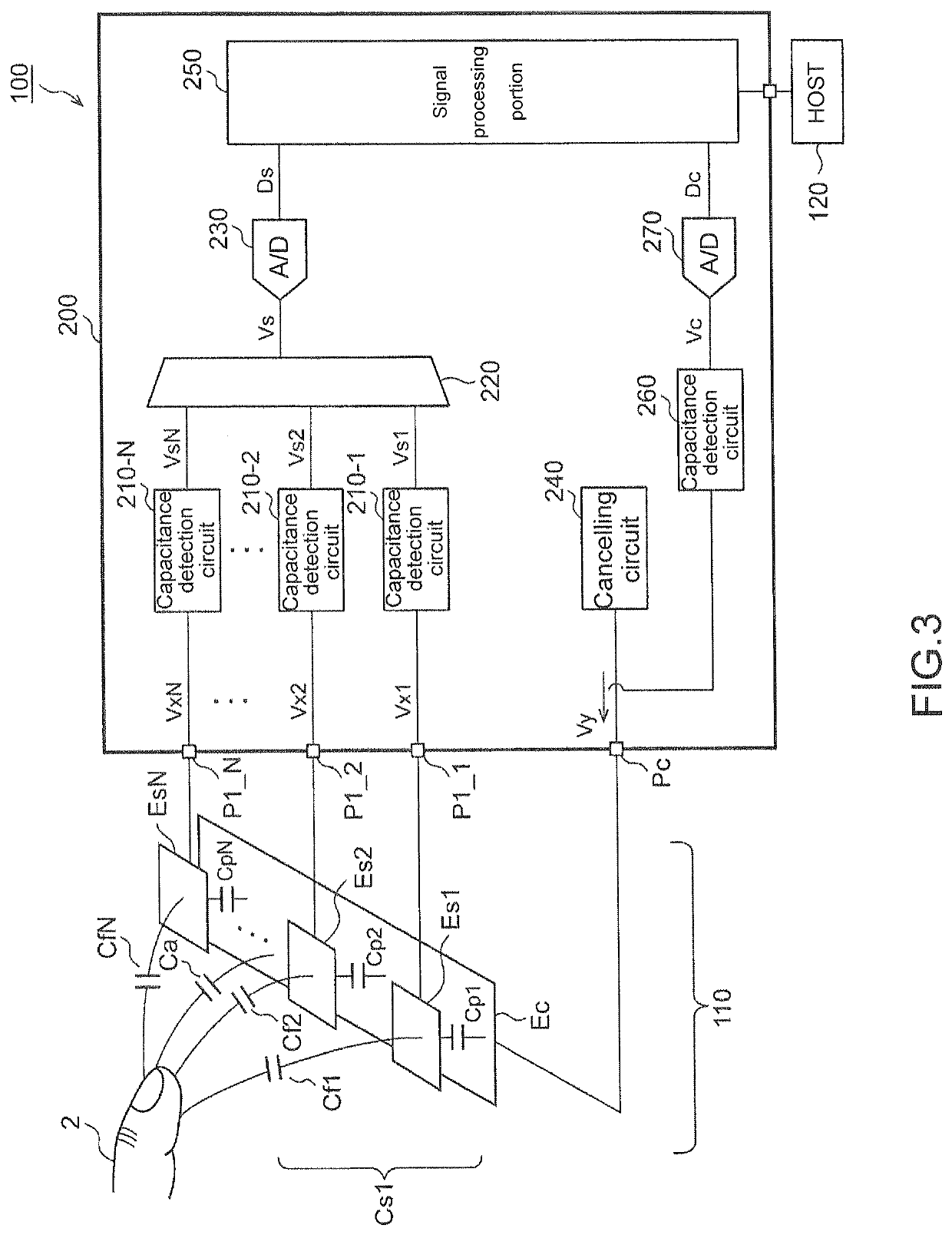
The present disclosure provides a touch detection circuit which comes with additional, new functions, an input device and an electronic apparatus.N first terminals (Ps) are each connected with a corresponding first electrode (Es). A second terminal (Pc) is connected with a second electrode (Ec). N first capacitance detection circuits (210) correspond to the N first terminals (Ps), change voltages of the first terminals (Ps), respectively, and each generate a first detection signal indicating an electrostatic capacitance of the corresponding first electrode (Es) in accordance with movement of a charge produced in the corresponding first terminal (Ps). A cancelling circuit (240) driving the second terminal (Pc) in a manner that a voltage of the second terminal (Pc) follows a voltage of the first terminal (Ps). A second capacitance detection circuit (260) generating a second detection signal indicating an electrostatic capacitance of the second electrode (Ec).

Description

BACKGROUND OF THE INVENTIONField of the Invention[0001]The present disclosure relates to a detection circuit of electrostatic capacitance.Description of the Prior Art[0002]In recent years, an electronic apparatus, such as a computer, smartphone, tablet terminal, and portable audio apparatus, uses a touch-style input device as a client interface. The touch-style input device, such as a conventional touch panel and a pointing device, receives various inputs by a user's finger, a stylus held by the user, or the user's approaching the touch-style input device.[0003]In general, the touch-style input devices come in two categories: resistance film style and electrostatic capacitance style. The electrostatic capacitance style involves converting variations in electrostatic capacitance (hereinafter abbreviated as capacitance) generated by a plurality of sensor electrodes into electrical signals according to a user's input, so as to detect for the presence of the user's input and coordinates...

Claims


Application Information

Patent Timeline
Patent Type & Authority Patents(United States)
IPC IPC(8): G06F3/045G06F3/041G06F3/044G01R27/26
CPCG06F3/044G01R27/2605G06F3/0416H03K17/962H03K17/9622H03K2217/96074H03K2217/960745H03K2217/960725H03K2217/960705
Inventor SHIMADA, YUJI
Owner ROHM CO LTD
Learn More