Collet inspection in a semiconductor pick and place apparatus

a technology of pick and place apparatus and pick and place, which is applied in the direction of gripping head, electrical apparatus, manipulator, etc., can solve the problems of mechanical parts expanding in the pick arm and errors during pick and place operations

Active Publication Date: 2021-07-06
ASMPT SINGAPORE PTE LTD
View PDF10 Cites 0 Cited by
  • Summary
  • Abstract
  • Description
  • Claims
  • Application Information

AI Technical Summary

Benefits of technology

[0010]The first aspect recognizes that pick and place apparatus are often operated for long periods of time at high transfer speeds, which may cause mechanical parts in the pick arm to expand due to the heat generated. The thermal expansion of the pick arm would cause its holding orifice to shift from its original position such that its position is no longer accurate or at the intended location, thus resulting in errors during pick and place operations. Accordingly, a pick and place apparatus is provided. The pick and place apparatus may be for manipulating semiconductor dice. The apparatus may comprise a pick arm. The pick arm may have a main body or component. The main body may define a conduit. The conduit may be located within the main body. The conduit may be configured to support a fluid flow through the main body using the conduit. The conduit may define a holding or vacuum orifice which may be used to secure or hold a semiconductor die. The conduit may be arranged to convey, propagate or transfer light which is received through the holding orifice on one side of the pick arm to an alignment window located on the main body on an opposite side of the pick arm. In this way, light can be used to illuminate the position of the holding orifice so that its location can be determined and corrected if necessary during the operation of the pick and place apparatus.
[0015]In one embodiment, the optical assembly seals the conduit at the optical assembly to prevent fluid communication between the ambient atmosphere and the conduit via the optical assembly. Sealing with the optical assembly improves the effectiveness of securing the semiconductor die to the holding orifice.
[0024]In one embodiment, at least one of the main body and the frusto-conical collet is dimensioned to extend along said major elongate axis such as to impair light transmission from the light source to the imaging device other than via the holding orifice. This helps to shield light other than light passing through the holding orifice from being received by the imaging device.
[0044]In one embodiment, the method comprises sealing the conduit at the optical assembly to prevent fluid communication between the ambient atmosphere and the conduit via the optical assembly.
[0053]In one embodiment, the method comprises dimensioning at least one of the main body and the frusto-conical collet to extend along said major elongate axis such as to impair light transmission from the light source to the imaging device other than via the holding orifice.

Problems solved by technology

The first aspect recognizes that pick and place apparatus are often operated for long periods of time at high transfer speeds, which may cause mechanical parts in the pick arm to expand due to the heat generated.
The thermal expansion of the pick arm would cause its holding orifice to shift from its original position such that its position is no longer accurate or at the intended location, thus resulting in errors during pick and place operations.

Method used


Image

  • Collet inspection in a semiconductor pick and place apparatus
  • Collet inspection in a semiconductor pick and place apparatus
  • Collet inspection in a semiconductor pick and place apparatus

Examples


Embodiment Construction

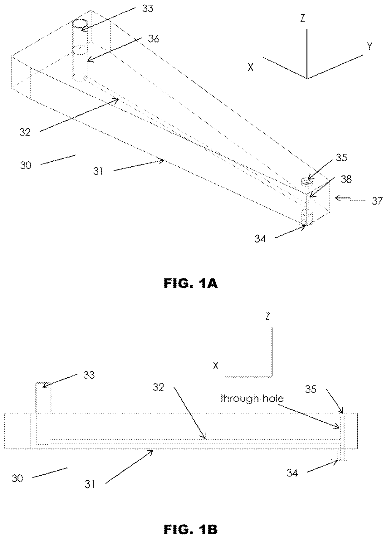
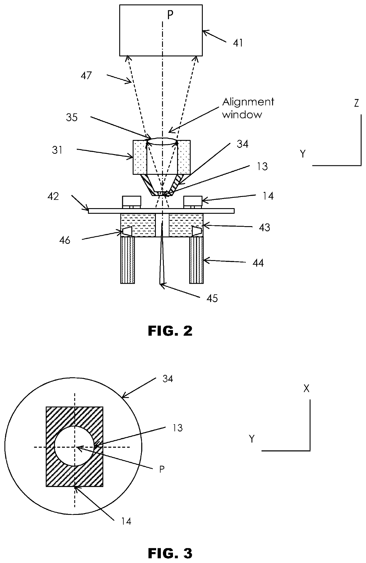
[0067]Before discussing the embodiments and more detail, first an overview will be provided. Embodiments provide an arm of a semiconductor pick and place apparatus which is configured to permit light to pass from a holding orifice of a conduit extending through the main body of the pick arm to be imaged by an imaging device so that its position can be accurately determined. The holding orifice needs to be accurately positioned to enable suction to be applied to a semiconductor die to hold the semiconductor die in place against the pick arm while being moved to a new location. In particular, light is projected from a surface or substrate on which a semiconductor die may be positioned, into the holding orifice and through the pick arm to be imaged by an imaging device. This enables the imaging device to determine the location of the holding orifice in relation to the imaging device, with the imaging device typically being aligned with the expected pick location of a semiconductor die ...


PUM

PropertyMeasurementUnit
vacuum suction forceaaaaaaaaaa
light transmissionaaaaaaaaaa
shapeaaaaaaaaaa

Abstract

A semiconductor pick and place apparatus comprises: a pick arm having a main body, and a conduit incorporated in the main body for permitting fluid flow through the main body via the conduit, the conduit further defining a holding orifice which is operative in use to secure a semiconductor die, the conduit being configured to convey light received from one side of the pick arm through the holding orifice and an alignment window located on the main body to an opposite side of the pick arm.

Description

FIELD OF THE INVENTION[0001]The invention relates to an apparatus and method for picking and placing semiconductors, such as for die sorting or die bonding applications.BACKGROUND[0002]A pick and place apparatus is used to pick up an object from a first station and thereafter to place or release the object at a second station. Pick and place devices are typically used in various semiconductor manufacturing processes, such as die bonding and die sorting.[0003]After a semiconductor wafer has been fabricated, the semiconductor wafer is usually mounted onto an adhesive film such as Mylar film, and subsequently singulated into individual semiconductor dice. The semiconductor dice may be tested either before or after singulation, in order to generate information for completing a wafer map containing characteristics of each semiconductor die together with its position in the wafer. The semiconductor dice may then be sorted based on the wafer map generated. A die sorting process may involve...

Claims


Application Information

Patent Timeline
Patent Type & Authority Patents(United States)
IPC IPC(8): H01L21/683B25J15/06B65G47/91H01L21/677
CPCH01L21/6838B25J15/0616B65G47/91H01L21/677H01L21/67144H01L21/681
Inventor LAM, KUI KAMLAM, KAI SIUTAM, CHEUK KIWONG, NIM TAKMAK, KA YEE
Owner ASMPT SINGAPORE PTE LTD
Why Eureka
Try Eureka