Touch panel and manufacturing method thereof

Active Publication Date: 2021-08-10
CAMBRIOS FILM SOLUTIONS CORP
View PDF7 Cites 0 Cited by
  • Summary
  • Abstract
  • Description
  • Claims
  • Application Information

AI Technical Summary

Benefits of technology

The patent text describes a method for creating metal patterns on a nanowire layer or metal layer without the need for additional steps. This simplifies the process and reduces production costs. Additionally, the method eliminates the need for alignment bit error areas, resulting in a narrower frame.

Problems solved by technology

However, these metal oxide films cannot meet the flexibility requirements of display devices.
However, there are still many problems to be solved in the nanowire process technology.
For example, most touch panel processes involve exposure development steps, and then undesired parts of the metal are removed according to the pattern.
The wire size of the peripheral area caused by the alignment bit error area cannot be reduced, thereby causing the width of the peripheral area to become larger.
Therefore, it cannot meet the narrow bezel requirements of displays.

Method used


Image

  • Touch panel and manufacturing method thereof
  • Touch panel and manufacturing method thereof
  • Touch panel and manufacturing method thereof

Examples


Embodiment Construction

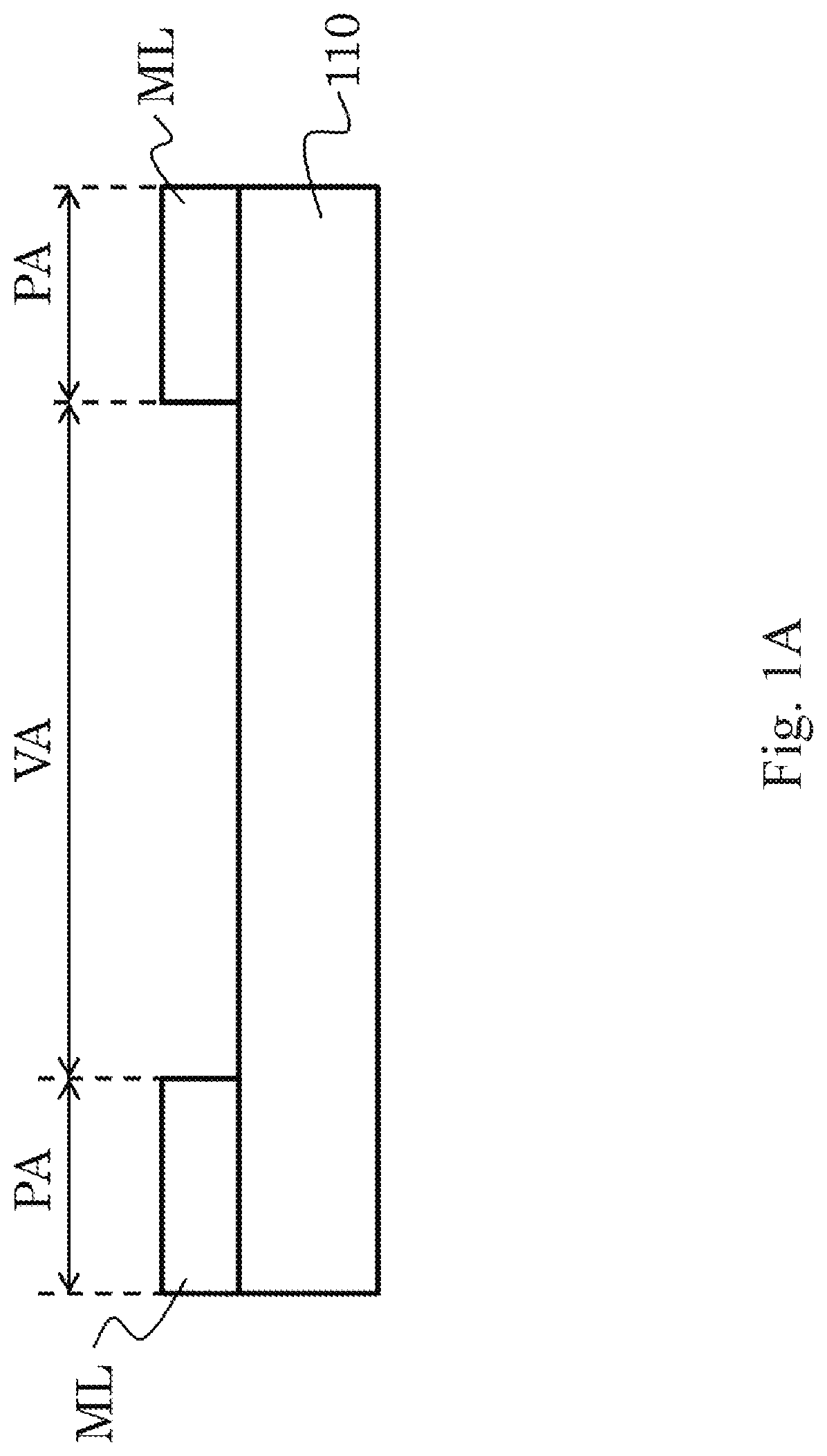
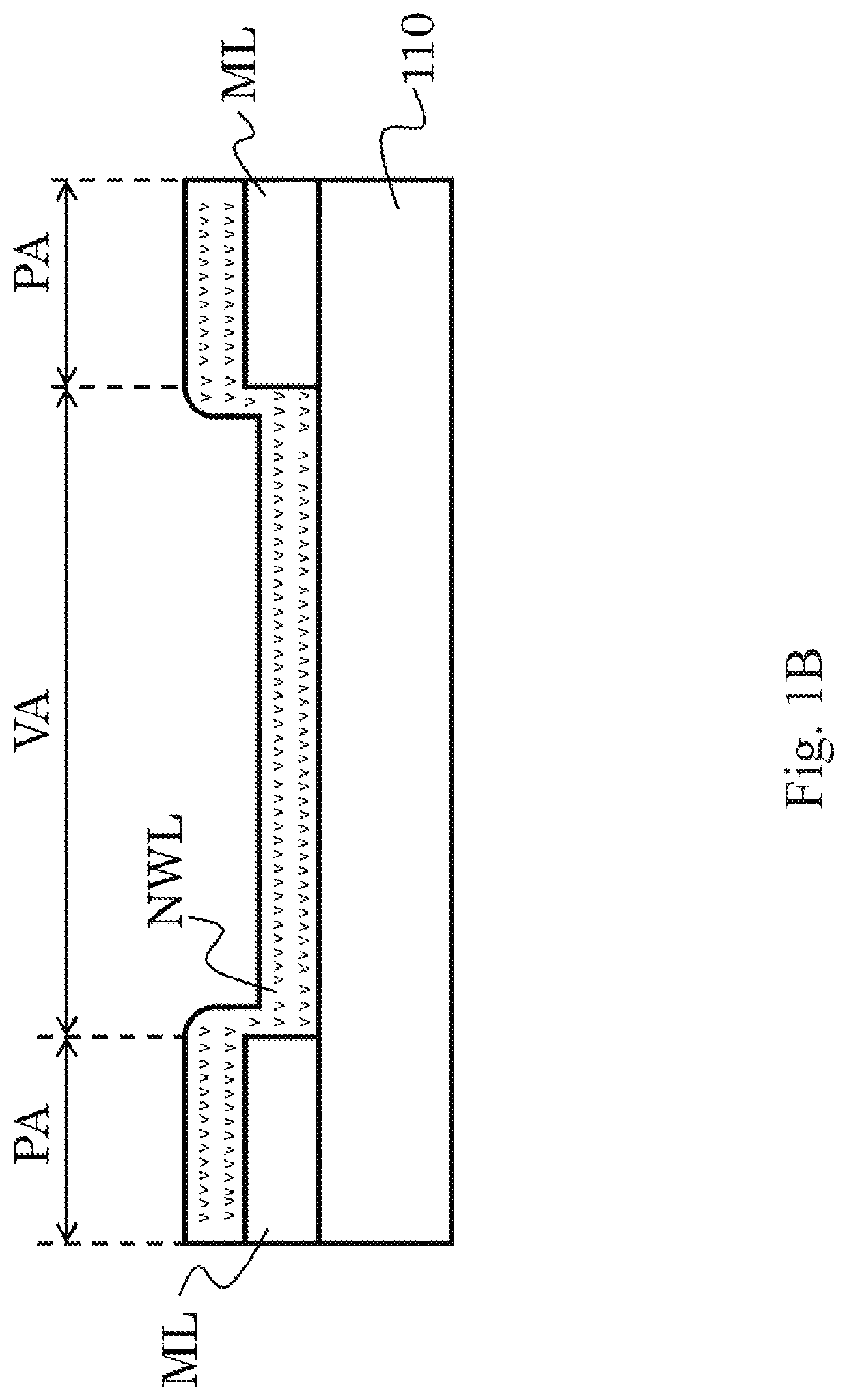
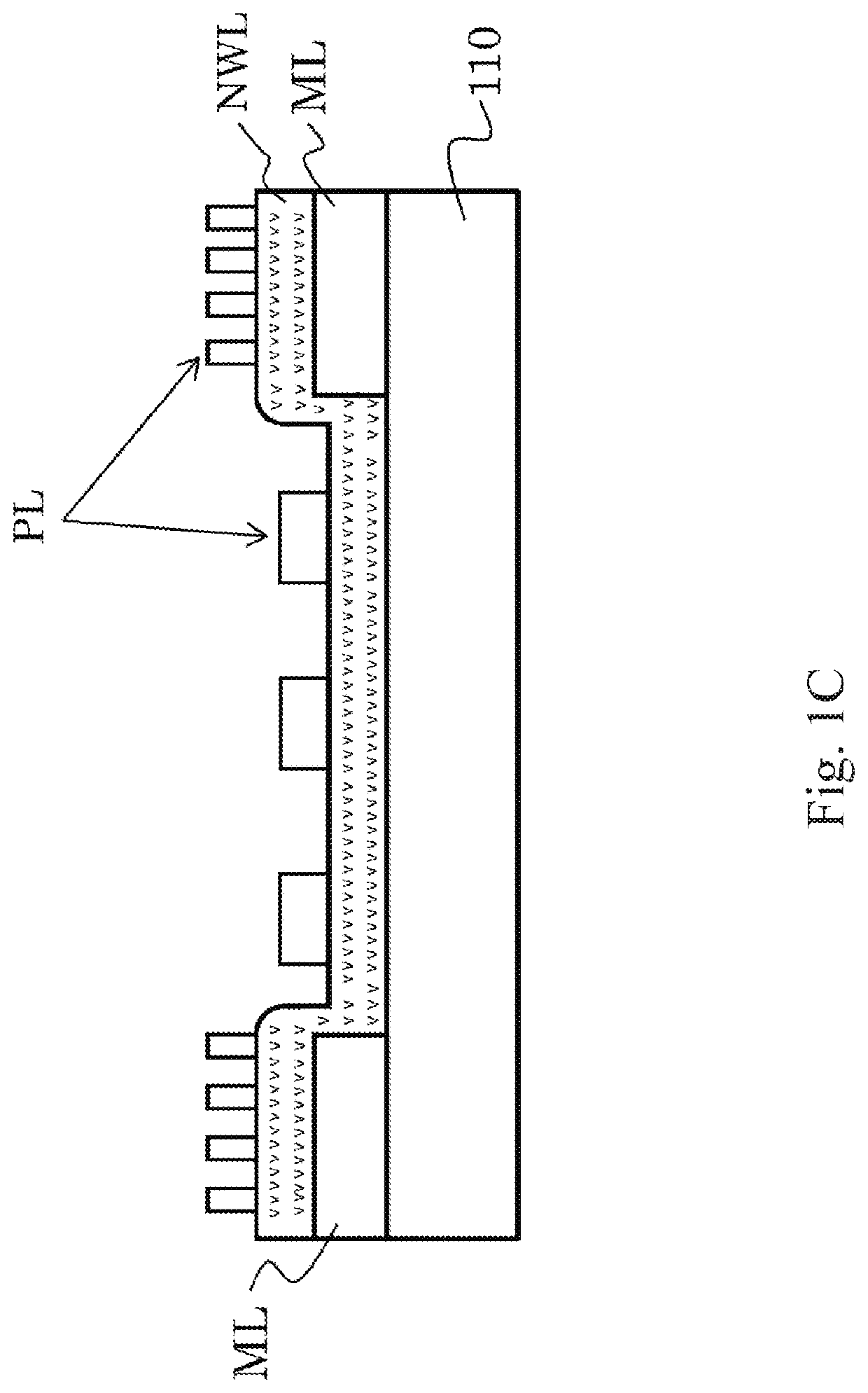
[0044]In the following, multiple embodiments of the present disclosure will be disclosed by drawings. Many practical details will be described in the following description for clarity. It should be understood, however, that these practical details should not be used to limit the disclosure. That is, in some embodiments of the present disclosure, these practical details are unnecessary. In addition, in order to simplify the drawings, some conventional structures and elements would be shown in the drawings in a simple and schematic manner.

[0045]Regarding “about”, “around” or “approximately” as used herein, the error or range of the value is generally indicated within 20%, preferably within 10%, and more preferably within 5%. Unless explicitly stated in the text, the mentioned values are regarded as approximate values, that is, they have errors or ranges as indicated by “about”, “around” or “approximately”.

[0046]Please refer to FIGS. 2 to 2B, which are a schematic top view and a schema...


PUM

PropertyMeasurementUnit
Structureaaaaaaaaaa

Abstract

A method of manufacturing a touch panel including providing a substrate having a display area and a peripheral area is provided. A metal layer and a metal nanowire layer are disposed, wherein a first portion of the metal nanowire layer is disposed in the display area, and a second portion of the metal nanowire layer and the metal layer are disposed in the peripheral area. A patterned layer with a pattern is disposed. A patterning step is performed according to the patterned layer, wherein the patterning step includes forming the metal layer into multiple peripheral wires and simultaneously forming the second portion of the metal nanowire layer into multiple etching layers by using an etching solution configured to etch the metal layer and the metal nanowire layer. A touch panel is further provided.

Description

CROSS-REFERENCE TO RELATED APPLICATION[0001]This application claims priority to China Application Serial Number 201910430058.2, filed May 22, 2019, which is herein incorporated by reference in its entirety.BACKGROUNDField of Disclosure[0002]The present disclosure relates to a touch panel and a manufacturing method thereof.Description of Related Art[0003]In recent years, transparent conductors have the characteristics of allowing light to pass through and simultaneously providing proper conductivity. Therefore, transparent conductors are often used in many display or touch-related devices. Generally, transparent conductors can be various metal oxides, for example, indium tin oxide (ITO), indium zinc oxide (IZO), cadmium tin oxide (CTO), or aluminum-doped zinc oxide (AZO). However, these metal oxide films cannot meet the flexibility requirements of display devices. Therefore, a variety of flexible transparent conductors have been developed, for example, transparent conductors made of ...

Claims


Application Information

Patent Timeline
IPC IPC(8): G06F3/041G06F3/044C23F1/02
CPCG06F3/0443C23F1/02G06F2203/04103G06F3/0412G06F3/0416C23F1/18C23F1/30C23C18/405C23C18/1608G06F3/04164
Inventor TSAI, YI-CHENFANG, WEI-CHIACHU, CHUN-HUNGHSIAO, CHUNG-CHIN
Owner CAMBRIOS FILM SOLUTIONS CORP
Why Eureka
Try Eureka