Semiconductor storage device and program method

a technology of semiconductors and storage devices, applied in the field of semiconductor storage devices, can solve the problems that the influence of capacitive coupling between adjacent bit lines cannot be ignored, and achieve the effect of lowering the current peak

Active Publication Date: 2021-09-14
WINBOND ELECTRONICS CORP
View PDF5 Cites 1 Cited by
  • Summary
  • Abstract
  • Description
  • Claims
  • Application Information

AI Technical Summary

Benefits of technology

[0004]In an NAND flash memory, a readout operation or a program operation is performed in pages, but when bit lines are distributed with narrow spacings due to increasing pages, the influence of capacitive coupling between the adjacent bit lines cannot be ignored. Therefore, one page is divided into ½ pages with an even page including even bit lines and an odd page including odd bit lines so as to make operations on the even page and the odd page different in time, so in appearance, distribution spacings between the bit lines are doubled, and the influence of capacitive coupling between the bit lines is restrained.
[0016]The disclosure is directed to solve the existing problems, and provides a program method capable of reducing a peak current of a program operation and a semiconductor device.

Problems solved by technology

In an NAND flash memory, a readout operation or a program operation is performed in pages, but when bit lines are distributed with narrow spacings due to increasing pages, the influence of capacitive coupling between the adjacent bit lines cannot be ignored.

Method used


Image

  • Semiconductor storage device and program method
  • Semiconductor storage device and program method
  • Semiconductor storage device and program method

Examples


Embodiment Construction

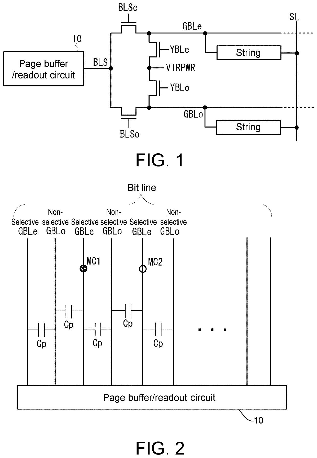
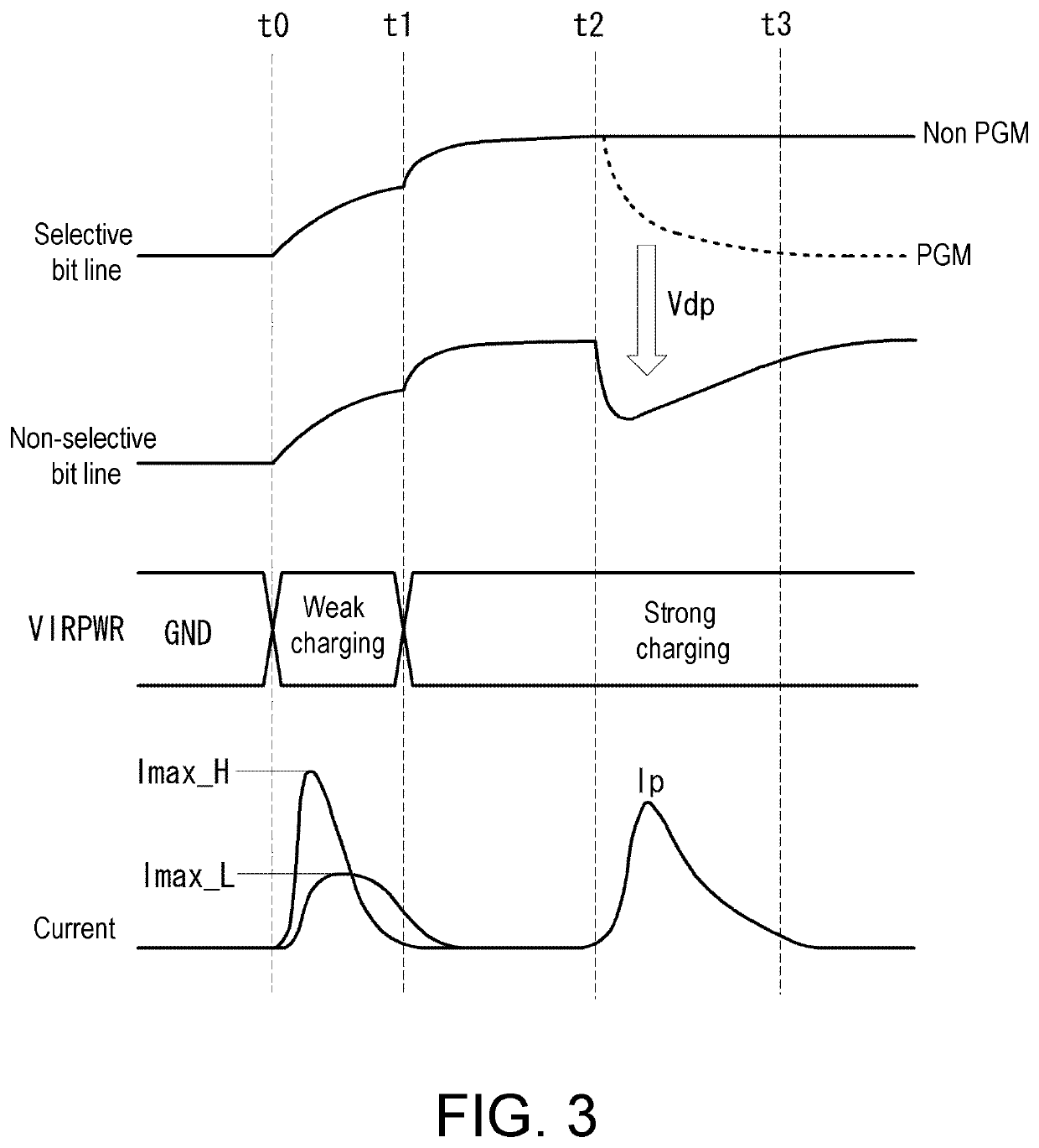
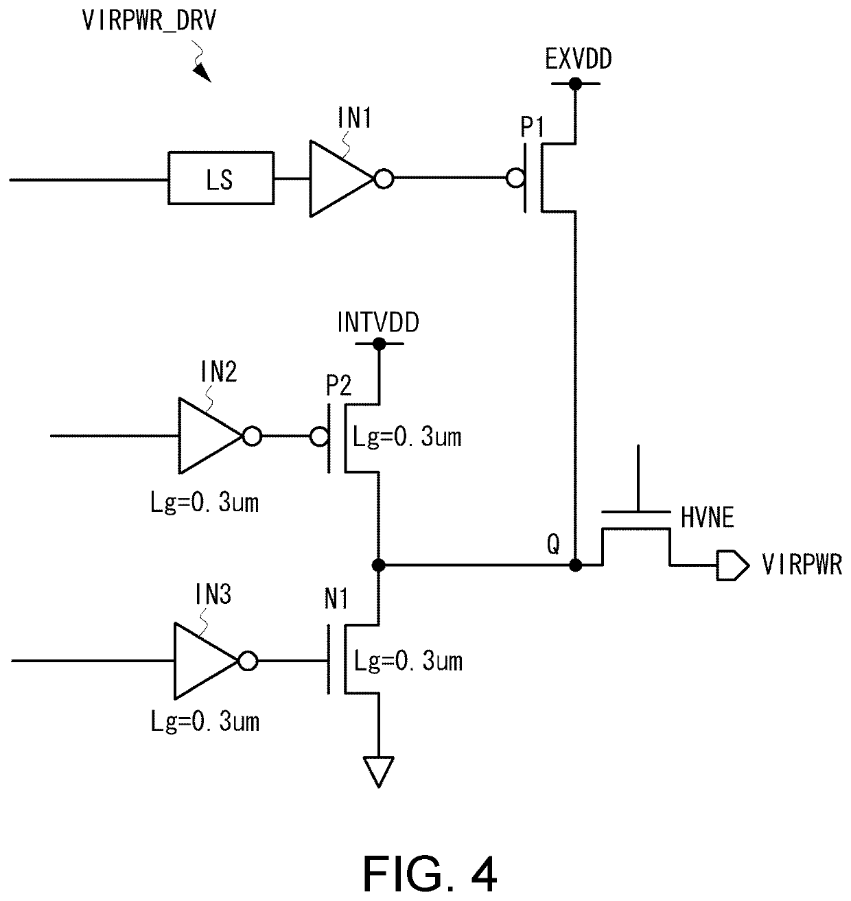
[0029]An implementation of the disclosure is illustrated below. In the implementation of the disclosure, a peak current is lowered in a program operation (e.g., a preset sequence is programmed) of an NAND flash memory. The peak current may be produced when voltage drop of bit lines is generated by the influence of capacitive coupling of the adjacent bit lines. Therefore, in the present implementation, the driving ability of a circuit driving the bit lines is regulated when voltage drop of the bit lines is produced so as to reduce the peak current in voltage drop of the bit lines without large compensation. The peak current of the disclosure is reduced during capacitive coupling of the adjacent bit lines, and during the period, the driving ability of the circuit driving the bit lines (e.g., a virtual voltage drive circuit) is switched from a strong driving ability to a weak driving ability.

[0030]Embodiments of the disclosure are illustrated in detail with reference to drawings below....


PUM


Abstract

A program method capable of reducing a peak current of a program operation is provided. The program method of a flash memory includes following steps: charging selective bit lines and non-selective bit lines by using a virtual voltage with weak driving ability during the time from t0 to t1 and a virtual voltage with strong driving ability during the time from t1 to t2, switching at least the non-selective bit lines to use the virtual voltage with weak driving ability for charging during at least the time from t2 to t3 when starting to discharge the selective bit lines connected to selective storage cells to a GND voltage level at time t2, and then applying program voltages to selective word lines.

Description

CROSS-REFERENCE TO RELATED APPLICATION[0001]This application claims the priority benefit of Japan application serial no. 2019-112184, filed on Jun. 17, 2019. The entirety of the above-mentioned patent application is hereby incorporated by reference herein and made a part of this specification.BACKGROUND OF THE INVENTION1. Field of the Invention[0002]The disclosure relates to a semiconductor storage device such as a flash memory, in particular to restraint of a peak current of a program operation.2. Description of Related Art[0003]In a readout operation of an NAND flash memory, pages including even bit lines or pages including odd bit lines are alternately read out. When even pages are being read out, odd pages are removed from a sense amplifier and provided with mask potentials, when the odd pages are being read out, the even pages are removed from the sense amplifier and provided with mask potentials, and therefore noise produced by capacitive coupling between adjacent bit lines is...

Claims


Application Information

Patent Timeline
Patent Type & Authority Patents(United States)
IPC IPC(8): G11C16/04G11C16/10G11C16/24G11C16/30
CPCG11C16/10G11C16/24G11C16/30G11C16/0483G11C16/26G11C16/32G11C16/08G11C7/12
Inventor OKABE, SHO
Owner WINBOND ELECTRONICS CORP
Why Eureka
Try Eureka