Semiconductor device with electrically connected doping regions and fabrication method thereof

a technology of semiconductor devices and doping regions, applied in semiconductor devices, semiconductor/solid-state device details, electrical apparatus, etc., can solve the problem of limited channel region length of individual finfets in fabrication processes

Active Publication Date: 2021-10-12
SEMICON MFG INT (SHANGHAI) CORP +1
View PDF15 Cites 1 Cited by
  • Summary
  • Abstract
  • Description
  • Claims
  • Application Information

AI Technical Summary

Benefits of technology

[0018]In the disclosed semiconductor device, the first conductive layers may be formed on the surfaces of the first source / drain doping regions. The total parallel resistance of the first conductive layers and the first source / drain doping regions may be less than the total parallel resistance of the first source / drain doping regions. Thus, when the semiconductor device is in operation, the dividing voltage on the first source / drain doping regions may be relatively small. Accordingly, under a constant voltage difference between the source voltages and the drain voltages, the total voltage for driving the gate structures to operate normally may be increased. Thus, more number of gate structures may be provided to control the channel regions of the transistors; and the design range of the number of the gate structures may be increased.
[0018]In the disclosed semiconductor device, the first conductive layers may be formed on the surfaces of the first source / drain doping regions. The total parallel resistance of the first conductive layers and the first source / drain doping regions may be less than the total parallel resistance of the first source / drain doping regions. Thus, when the semiconductor device is in operation, the dividing voltage on the first source / drain doping regions may be relatively small. Accordingly, under a constant voltage difference between the source voltages and the drain voltages, the total voltage for driving the gate structures to operate normally may be increased. Thus, more number of gate structures may be provided to control the channel regions of the transistors; and the design range of the number of the gate structures may be increased.
[0008]Another aspect of the present disclosure includes a method for forming a semiconductor device. The method includes providing a base substrate; forming a gate structure group, having a plurality of gate structures, over the base substrate; forming first source / drain doping regions in the base substrate between adjacent gate structures and second source / drain doping regions in the base substrate at two sides of the gate structure group, respectively; and forming a first conductive layer on a surface of each of first source / drain doping regions. The second source / drain doing regions at one side of the gate structure group are electrically connected with source voltages; and the second source / drain doping regions at the other side of the gate structure group are electrically connected with drain voltages.

Problems solved by technology

However, the length of the channel region of an individual FinFET is limited by the fabrication process.

Method used


Image

  • Semiconductor device with electrically connected doping regions and fabrication method thereof
  • Semiconductor device with electrically connected doping regions and fabrication method thereof
  • Semiconductor device with electrically connected doping regions and fabrication method thereof

Examples


Embodiment Construction

[0014]Reference will now be made in detail to exemplary embodiments of the disclosure, which are illustrated in the accompanying drawings. Wherever possible, the same reference numbers will be used throughout the drawings to refer to the same or like parts.

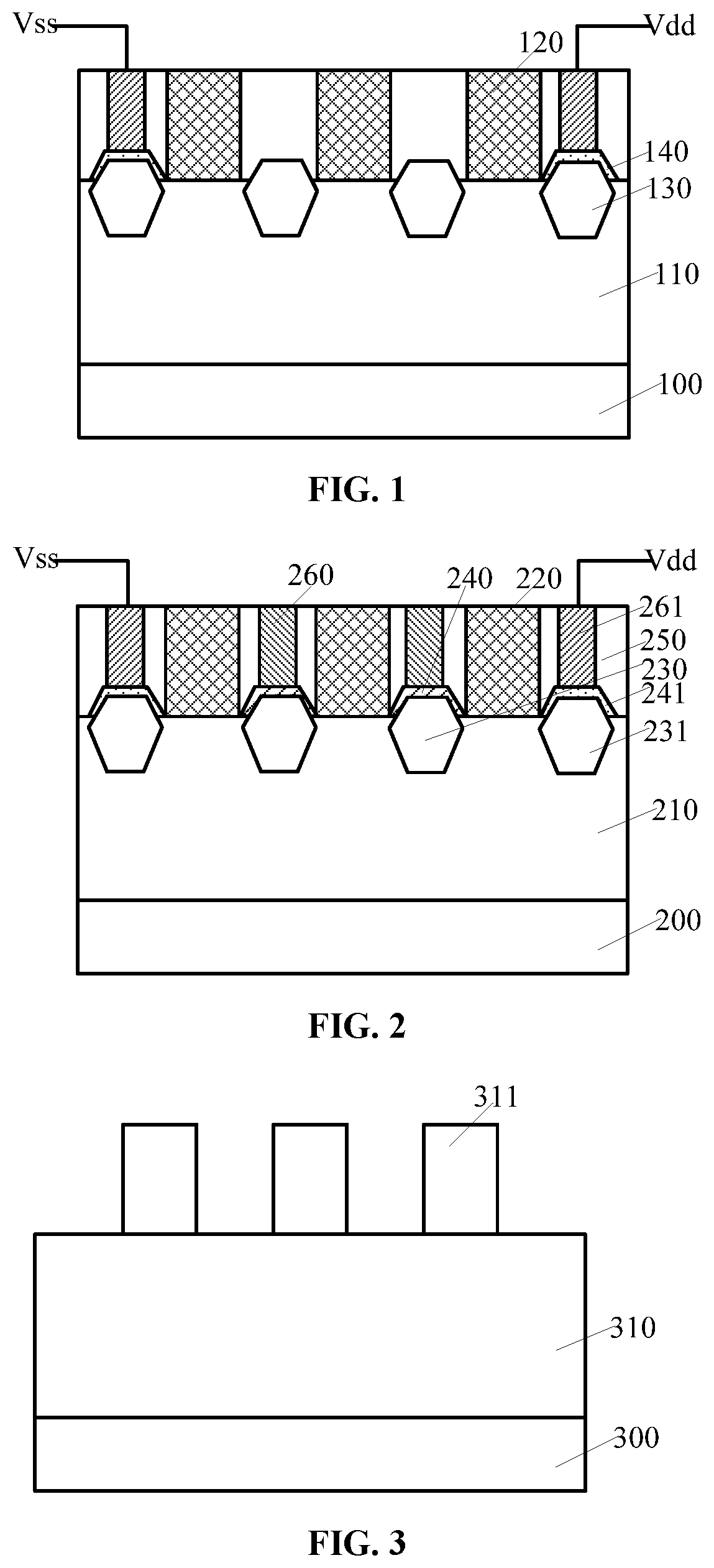
[0015]FIG. 1 illustrates a semiconductor device having a plurality of fins connected in serial. The semiconductor device includes a semiconductor substrate 100; a plurality of fins 110 on the semiconductor substrate 100; a gate structure group having a plurality gate structures 120 crossing over the fins 110 and covering portions of the side and top surfaces of the fins 110; source / drain doping regions 130 formed in the fins 110 at two sides of the gate structure group; and metal silicide layers 140 formed on the surfaces of the source / drain doping regions 130 at the two sides of the gate structure group. The metal silicide layers 140 at one side of the gate structure group are electrically connected with source voltages Vss; and ...


PUM

PropertyMeasurementUnit
conductiveaaaaaaaaaa
source voltageaaaaaaaaaa
drain voltageaaaaaaaaaa

Abstract

Semiconductor devices and fabrication methods thereof are provided. An exemplary semiconductor device includes a base substrate; a gate structure group, having a plurality of gate structures, formed over the base substrate; first source / drain doping regions formed in the base substrate between adjacent gate structures; second source / drain doping regions formed in the base substrate at two sides of the gate structure group, respectively; a first conductive layer formed on a surface of each of the first source / drain doping regions. The second source / drain doing regions at one side of the gate structure group are electrically connected with source voltages; and the second source / drain doping regions at other side of the gate structure group are electrically connected with drain voltages.

Description

CROSS-REFERENCES TO RELATED APPLICATIONS[0001]This application claims the priority of Chinese patent application No. 201610961821.0, filed on Nov. 4, 2016, the entirety of which is incorporated herein by reference.FIELD OF THE DISCLOSURE[0002]The present disclosure generally relates to the field of semiconductor manufacturing technologies and, more particularly, relates to semiconductor devices and fabrication methods thereof.BACKGROUND[0003]MOS transistors are one of the most important types of components in modern integrated circuits (ICs). The basic structure of an MOS transistor includes a semiconductor substrate, a gate structure on the surface of the semiconductor substrate; a source region in the semiconductor substrate at one side of the gate structure and a drain region in the semiconductor substrate at another side of the gate structure. The basic principle of the MOS transistor is to apply a bias on the gate structure to control the current in the channel region under the...

Claims


Application Information

Patent Timeline
Patent Type & Authority Patents(United States)
IPC IPC(8): H01L21/02H01L29/45H01L29/417H01L29/78H01L29/66H01L21/8234H01L23/535H01L27/088H01L29/08
CPCH01L29/456H01L21/823418H01L21/823431H01L21/823475H01L23/535H01L27/0886H01L29/0847H01L29/41791H01L29/66795H01L29/785
Inventor ZHOU, FEI
Owner SEMICON MFG INT (SHANGHAI) CORP
Why Eureka
Try Eureka