Static random access memory (SRAM) bit cells employing asymmetric width read and write word lines, and related methods

a random access memory and bit cell technology, applied in the field of memory for computer systems for reading and writing data, can solve the problems of over-all desired memory access latency, achieve the effects of reducing memory write latency, improving memory write access performance, and increasing the width of the write word lin

Active Publication Date: 2022-01-11
QUALCOMM INC
View PDF6 Cites 1 Cited by
  • Summary
  • Abstract
  • Description
  • Claims
  • Application Information

AI Technical Summary

Benefits of technology

[0005]Aspects disclosed herein include static random access memory (SRAM) bit cells employing an asymmetric width read and write word lines. Related fabrication methods are also disclosed. SRAM bit cells employing asymmetric width read and write word lines can reduce memory write latency and improve memory write access performance. The SRAM bit cell can be provided in the form of a complementary metal oxide semiconductor (CMOS) circuit in a cell circuit according to a circuit cell design layout in an example. The routing area provided for the layout of the write word line and read word line in the circuit cell for the SRAM bit cell is based on the design rule constraints for the SRAM bit cell. In exemplary aspects disclosed herein, the SRAM bit cell employs an increased width write word line based on a circuit cell layout area savings achieved by employing a reduced width read word line. Increasing the width of the write word line can reduce the resistance of the write word line and decrease memory write latency to the SRAM bit cell as a result. In certain exemplary aspects, the metal line pitch and minimum distance between metal lines of the SRAM bit cell can be maintained for maintaining fabrication compatibility with existing fabrication processes with decreasing the resistance of the write word line of the SRAM bit cell. Decreasing the width of the read word line to allow an increased width write word line may not compromise read access latency sufficiently to affect the overall desired memory access latency of the SRAM bit cell in an intolerable manner. In some examples, the SRAM bit cell includes multiple read word lines having a smaller width than one or more write word lines based on the number of read and write ports provided for the SRAM bit cell.
[0006]In other exemplary aspects, the read word line of the SRAM bit cell is provided in a higher metal layer than the write word line in the SRAM bit cell in an integrated circuit (IC). The metal layer in which the write word line is disposed includes a read word line interconnect that is coupled to the read word line in the higher metal layer through one or more read word line interconnect vertical interconnect accesses (vias). The read word line interconnect via connected to the read word line interconnect is larger in at least one dimension (e.g., width) than a write word line via that interconnects the write word line to a lower metal layer and / or transistor of the SRAM bit cell. Increasing the size of the read word line interconnect via can mitigate any increased resistance that may be present in the read word line as a result of decreasing the width of the read word line interconnect. The read word line interconnect may be enlarged in width to accommodate a connection with the full area of the enlarged read word line interconnect via.

Problems solved by technology

Decreasing the width of the read word line to allow an increased width write word line may not compromise read access latency sufficiently to affect the overall desired memory access latency of the SRAM bit cell in an intolerable manner.

Method used


Image

  • Static random access memory (SRAM) bit cells employing asymmetric width read and write word lines, and related methods
  • Static random access memory (SRAM) bit cells employing asymmetric width read and write word lines, and related methods
  • Static random access memory (SRAM) bit cells employing asymmetric width read and write word lines, and related methods

Examples


Embodiment Construction

[0027]With reference now to the drawing figures, several exemplary aspects of the present disclosure are described. The word “exemplary” is used herein to mean “serving as an example, instance, or illustration.” Any aspect described herein as “exemplary” is not necessarily to be construed as preferred or advantageous over other aspects.

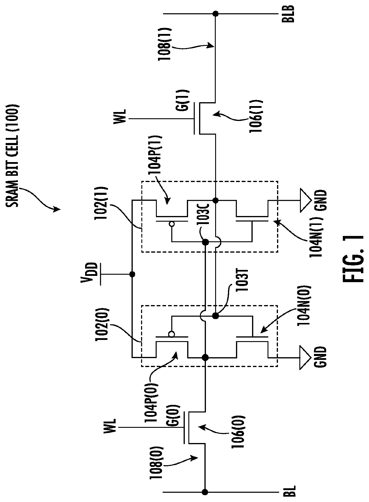
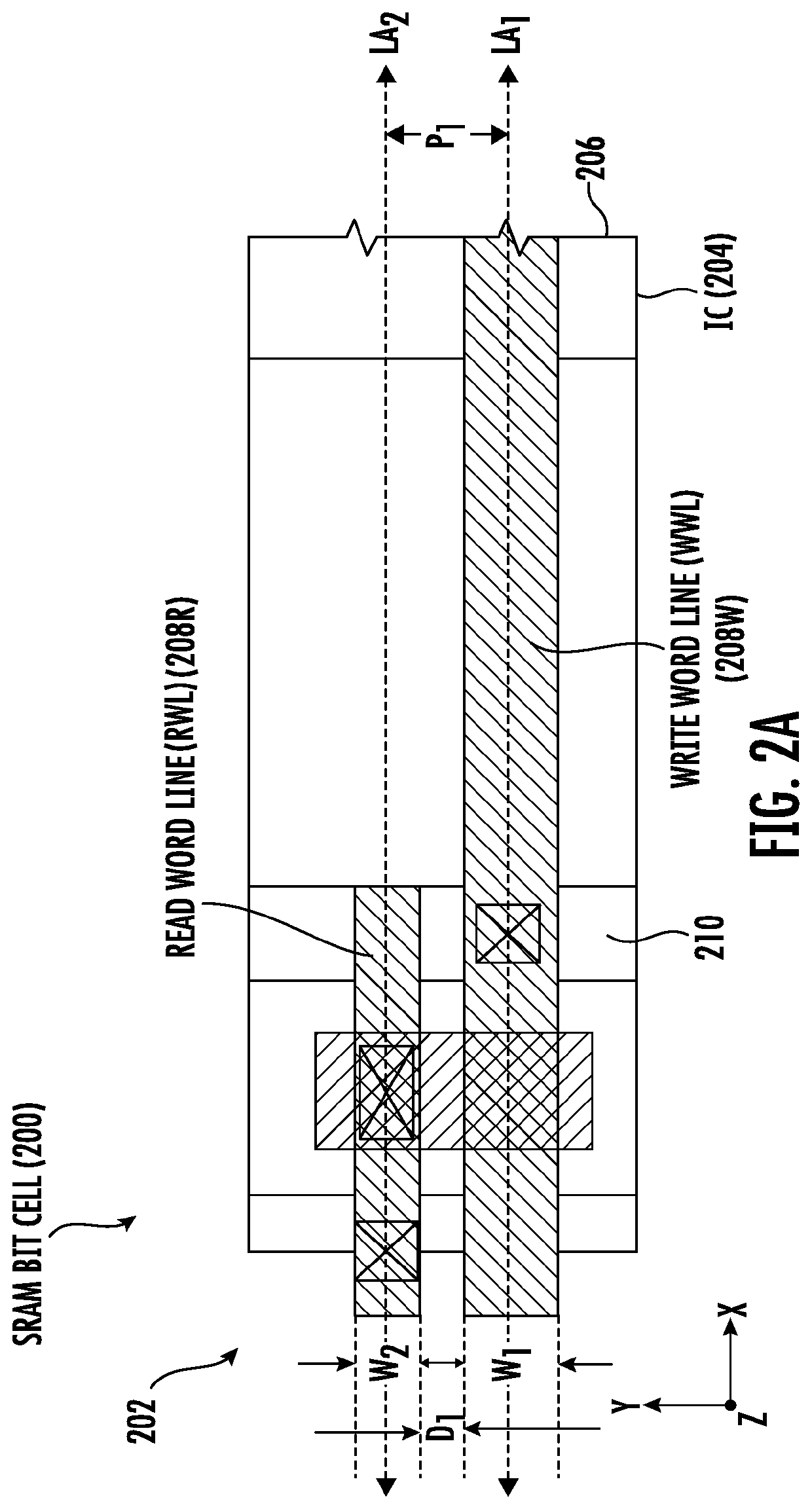
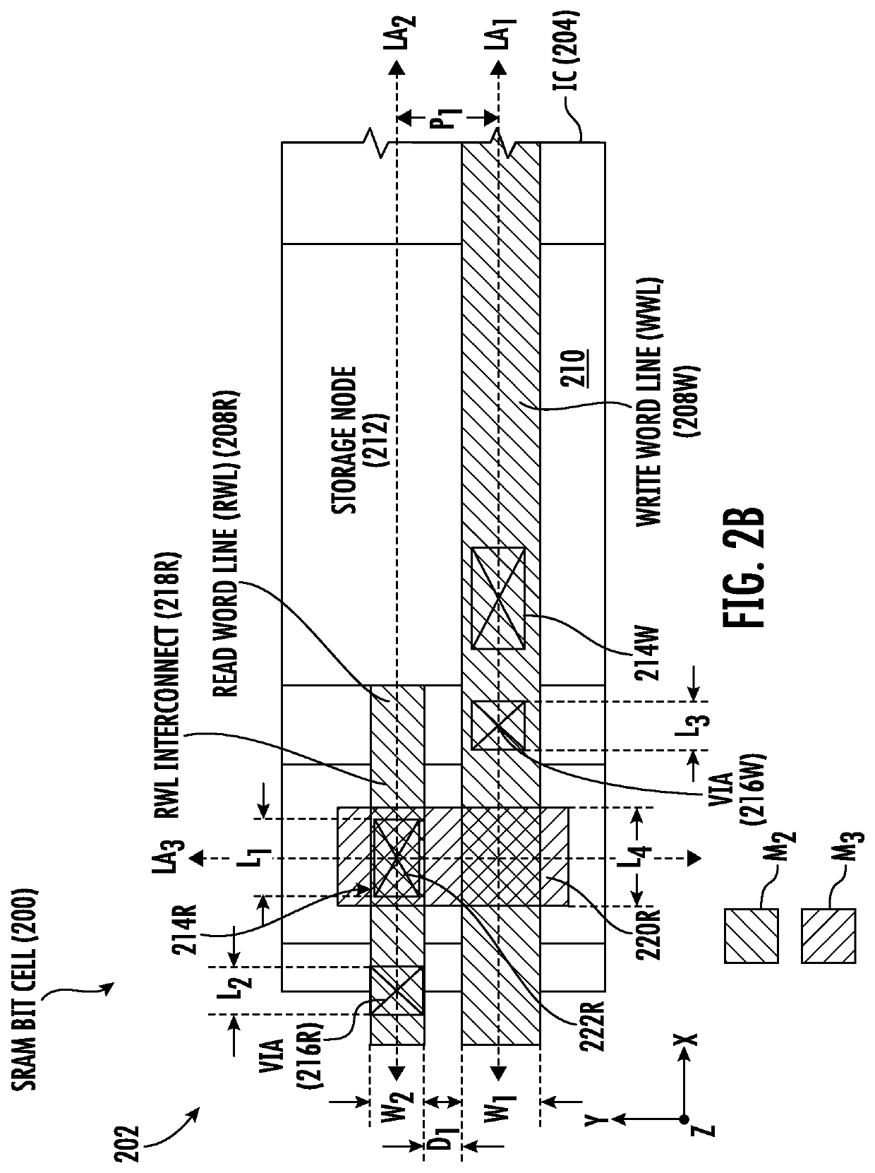
[0028]Aspects disclosed herein include static random access memory (SRAM) bit cells employing an asymmetric width read and write word lines. Related fabrication methods are also disclosed. SRAM bit cells employing asymmetric width read and write word lines can reduce memory write latency and improve memory write access performance. The SRAM bit cell may be provided in the form of a complementary metal oxide semiconductor (CMOS) circuit in a cell circuit according to a circuit cell design layout in an example. The routing area provided for the layout of the write word line and read word line in the circuit cell for the SRAM bit cell is based on the des...


PUM


Abstract

Static random access memory (SRAM) bit cells employing asymmetric width read and write word lines (WWL) for reduced memory write latency and improved memory write access performance, and related fabrication methods are disclosed. In exemplary aspects, the SRAM bit cell employs an increased width write word line based on a circuit cell layout area savings achieved by employing a reduced width read word line. Increasing the width of the write word line can reduce the resistance of the write word line and decrease memory write latency to the SRAM bit cell as a result. In certain exemplary aspects, the metal line pitch and minimum distance between metal lines of the SRAM bit cell can be maintained for maintaining fabrication compatibility with existing fabrication processes with decreasing the resistance of the write word line of the SRAM bit cell.

Description

BACKGROUNDI. Field of the Disclosure[0001]The technology of the disclosure relates generally to memory for computer systems for reading and writing data, and particularly to memory employing static random access memory (SRAM) bit cells.II. Background[0002]Processor-based computer systems include memory for data storage. Different types of memory exist that each possessing certain unique features. For example, static random access memory (SRAM) is a type of memory that can be employed in processor-based computer systems. SRAM can store data without the need to periodically refresh the memory, unlike dynamic random access memory (DRAM) for example. An SRAM contains a plurality of SRAM bit cells (also referred to as “bit cells”) organized in memory rows and columns in an SRAM array. For any given row in an SRAM array, each column of the SRAM array includes an SRAM bit cell in which a single data value or bit is stored. Memory read and write operations are performed on a particular SRAM...

Claims


Application Information

Patent Timeline
Patent Type & Authority Patents(United States)
IPC IPC(8): H01L23/528H01L27/11H01L21/8238H01L21/768H01L23/522
CPCH01L23/5283H01L21/76816H01L21/76877H01L21/823871H01L23/5226H01L27/1104H01L27/1116
Inventor SHARMA, SUNILBIRADAR, RAHULGHOSH, SONIA
Owner QUALCOMM INC
Why Eureka
Try Eureka