Piezoelectric transformer
a technology of piezoelectric transformer and film thickness, which is applied in the direction of piezoelectric/electrostrictive/magnetostrictive devices, piezoelectric/electrostrictive/magnetostriction machines, mechanical vibration separation, etc., can solve the problems of degrading conversion efficiency, degrading power transmission efficiency of piezoelectric transformer, and difficult manufacturing of film thickness and material changes of piezoelectric bodies. achieve the effect of large voltage and high transformation ratio
- Summary
- Abstract
- Description
- Claims
- Application Information
AI Technical Summary
Benefits of technology
Problems solved by technology
Method used
Image


Examples
embodiment 1
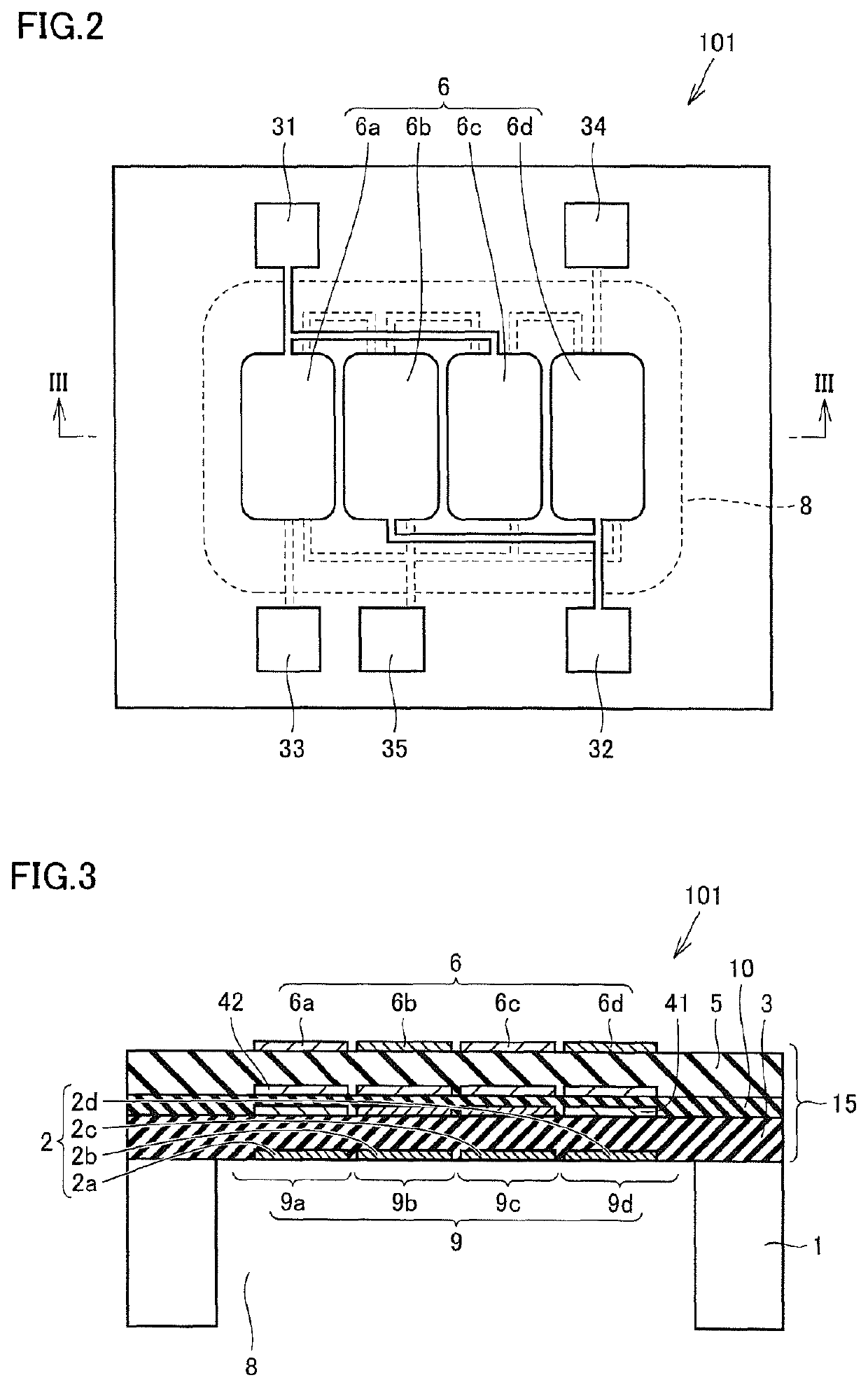
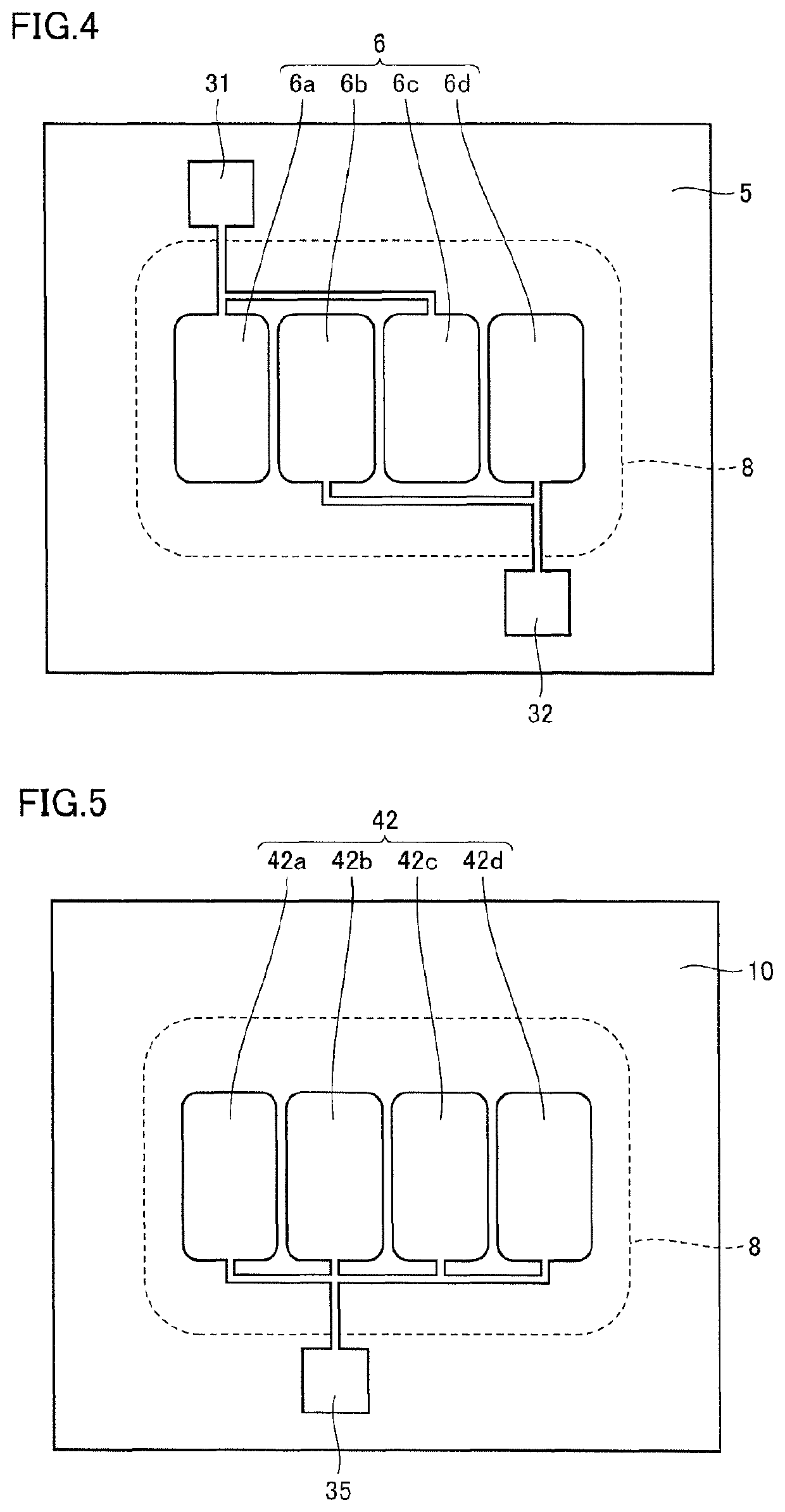
[0043]A piezoelectric transformer according to embodiment 1 of the present invention will be described while referring to FIGS. 1 to 8. FIG. 1 illustrates the exterior of a piezoelectric transformer 101 of this embodiment. FIG. 2 illustrates a plan view of the piezoelectric transformer 101. FIG. 3 illustrates a sectional view looking in the direction of the arrows and taken along line III-III in FIG. 2. FIGS. 4 to 7 illustrate the layouts of conductor patterns and so forth of layers included in the piezoelectric transformer 101. FIG. 8 illustrates a conceptual diagram in which a vibration film of the piezoelectric transformer 101 is illustrated together with related wiring lines.
[0044]As illustrated in FIG. 1, the piezoelectric transformer 101 includes a base 1 and an upper layer 15 that is supported by the base 1. The base 1 may be a member composed of Si, for example. The base 1 is not limited to being a plate-shaped member, and may be formed using a plate-shaped member. For examp...
embodiment 2
[0078]A piezoelectric transformer according to embodiment 2 of the present invention will be described while referring to FIGS. 10 to 13. FIG. 10 illustrates the exterior of a piezoelectric transformer 102 of this embodiment. FIG. 11 illustrates a plan view of the piezoelectric transformer 102. FIG. 12 illustrates the layout of an input electrode 6 and so forth on the upper surface of a second piezoelectric layer 5 included in the piezoelectric transformer 102. The layout of the conductor patterns and so forth of the other layers are the same as illustrated in FIGS. 5 to 7 in embodiment 1. FIG. 13 illustrates a conceptual diagram in which a vibration film of the piezoelectric transformer 102 is illustrated together with related wiring lines.
[0079]As illustrated in FIG. 10, the piezoelectric transformer 102 includes a base 1 and an upper layer 15 that is supported by the base 1. The details of the base 1 are the same as described in embodiment 1. The upper layer 15 includes a vibrati...
embodiment 3
[0087]A piezoelectric transformer according to embodiment 3 of the present invention will be described while referring to FIGS. 15 to 20. FIG. 15 illustrates a plan view of a piezoelectric transformer 103 according to this embodiment. FIGS. 16 to 19 illustrate the layouts of conductor patterns and so forth of layers included in the piezoelectric transformer 103. FIG. 20 illustrates a conceptual diagram in which a vibration film of the piezoelectric transformer 103 is illustrated together with related wiring lines.
[0088]The piezoelectric transformer 103 corresponds to a case in which n=2 in the piezoelectric transformer 101 described in embodiment 1. In other words, as illustrated in FIG. 20, the vibration portion assembly 9 includes two vibration portions 9a and 9b. The input electrode 6 includes one to n input electrode pieces 6a and 6b that are arrayed in a divided manner so as to correspond to at least some of the n, i.e., two vibration portions 9a and 9b. The output electrode 2 ...
PUM
 Abstract
Description
Claims
Application Information
 - R&D
- Intellectual Property
- Life Sciences
- Materials
- Tech Scout
- Unparalleled Data Quality
- Higher Quality Content
- 60% Fewer Hallucinations
Browse by: Latest US Patents, China's latest patents, Technical Efficacy Thesaurus, Application Domain, Technology Topic, Popular Technical Reports.
© 2025 PatSnap. All rights reserved.Legal|Privacy policy|Modern Slavery Act Transparency Statement|Sitemap|About US| Contact US: help@patsnap.com