Photocoupler

a photocoupler and photoelectric technology, applied in the field of electromechanical components, can solve the problems of not all products are capable of meeting the requirements of high voltage resistance, the production of thin-series photocouplers is either in poor production yield or with high defective products, and achieves easy forming, reduce parasitic capacitance of products, and improve common-mode interference immunity.

Active Publication Date: 2022-02-15
CT MICRO INT
View PDF11 Cites 0 Cited by
  • Summary
  • Abstract
  • Description
  • Claims
  • Application Information

AI Technical Summary

Benefits of technology

[0004]Therefore, an objective of the present invention is to provide a photocoupler of which the manufacturing process is simpler, the inner encapsulant body and the outer encapsulant are easily shaped, the structure design is thinner, the specification meets safety requirement, and light transmission efficiency is better than that of the photocouplers with the packaging structure of opposite arrangement.
[0012]By the technical means adopted by the present invention, the light-reflecting encapsulant body and the light-transmissive encapsulant body are formed by double molding and epoxy molding. The light-transmissive encapsulant body is easily shaped during manufacturing process. According to the required optical characteristics, a mold can be performed by a special processing and a surface treatment so that the light-transmissive encapsulant body is able to be shaped into a corresponding shape. The light-reflective encapsulant body encloses the light-transmissive encapsulant body and reflects the light emitted from the light-emitting chip.
[0013]Furthermore, comparing to the structure that the light-emitting chip and the light-sensing chip are disposed face to face, the present invention provides the light-emitting chip and the light-sensing chip being disposed side by side in a coplanar manner, which can effectively reduce the parasitic capacitance of the products to enable the products to have higher common-mode interference immunity. Besides, such kind of packaging structure has lower process difficulty, avoids risk of failure due to poor production control for product manufacture, and can greatly improve the high-voltage resistant performance and stability for the photocoupler. The photocoupler of the present invention not only meets the safety regulation of metal penetration distance but greatly lowers the size of the photocoupler, thereby meeting market demand for thinner design.
[0014]Moreover, in embodiments, the light-emitting surface of the light-emitting chip and the light-receiving surface of the light-sensing chip face toward the mounting direction. When the photocoupler of the present invention is mounted on a circuit board, the light-emitting surface of the light-emitting chip and the light-receiving surface of the light-sensing chip face the circuit board in such a manner that the amount of light transmitted from the outside of the light-reflective encapsulant body into the light-transmissive encapsulant body can be reduced by the shielding of the printed circuit board so as to prevent the light-sensing chip from the interference of external light and enable the photocoupler to be used in an environment filled with an interference of high density light source.

Problems solved by technology

A requirement of high voltage resistance for photocoupler is in necessity, so in a packaging process that the light-emitting chip and light-sensing chip are oppositely disposed, the alignment accuracy between the light-emitting chip and light-sensing chip is difficult to achieve such that not all products are capable of meeting the requirement of high voltage resistance.
The above requirement leads a complicated manufacturing process to cause the production of thin series photocouplers to be either in poor production yield or with high defective products.
A packaging structure of opposite arrangement also causes the photocoupler to have high capacitance characteristic such that, in terms of the common mode rejection noise characteristic, more additional design and cost are required for the photocoupler to avoid the interference of common mode voltage.
Furthermore, although the photocouplers have been widely used in various electrical products, the characteristic of the photocouplers are unable to meet application needs since an inner encapsulant body and an outer encapsulant body in the conventional photocouplers are difficult to be shaped and a tight attachment is difficult to be formed between the inner encapsulant body and the outer encapsulant body.

Method used


Image

  • Photocoupler
  • Photocoupler
  • Photocoupler

Examples


Embodiment Construction

[0022]The preferred embodiments of the present invention are described in detail below with reference to FIG. 1 to FIG. 7. The description is used for explaining the embodiments of the present invention only, but not for limiting the scope of the claims.

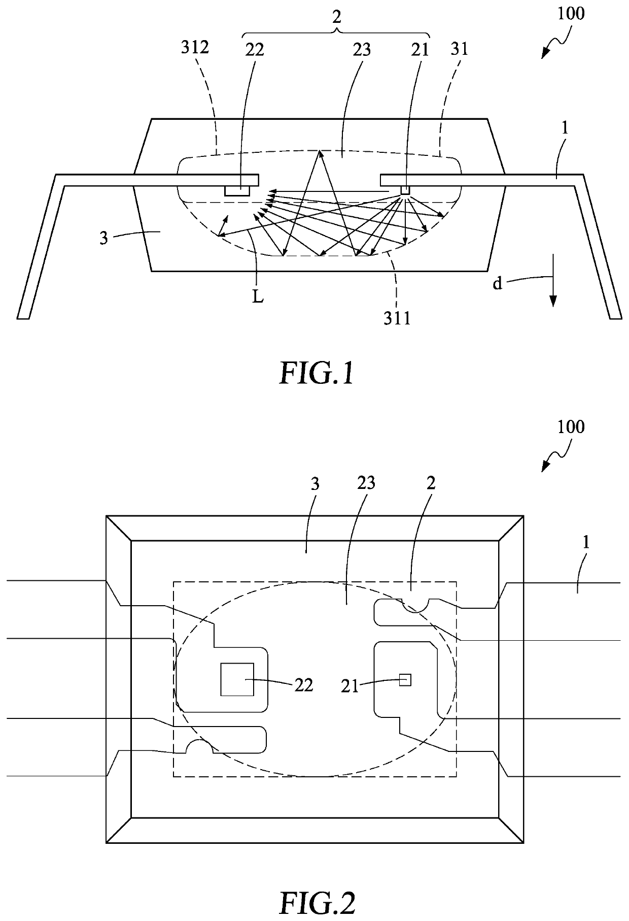
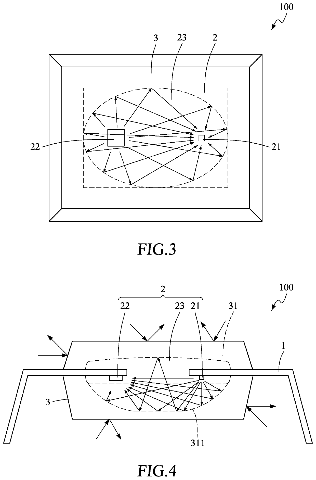
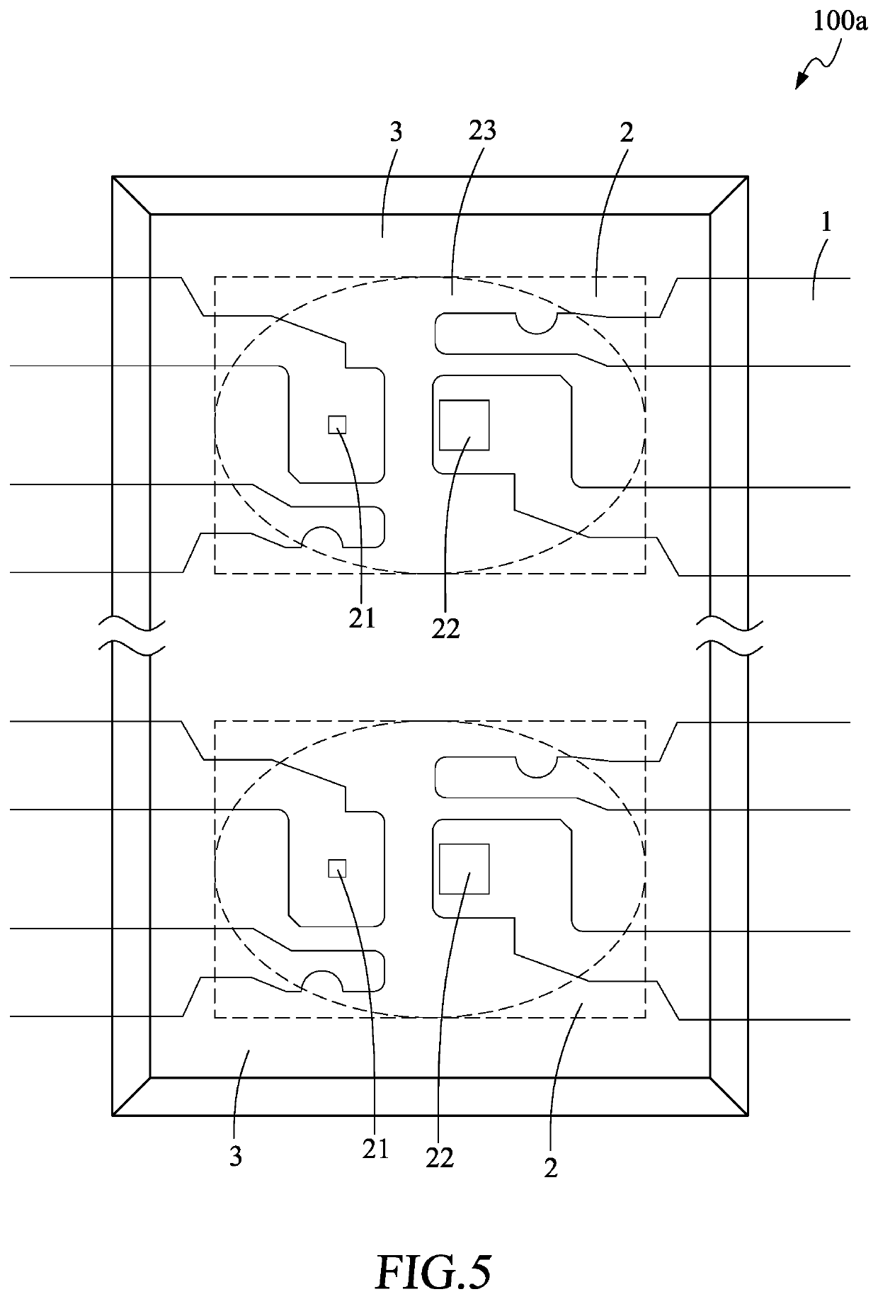
[0023]As shown in FIG. 1 to FIG. 4, a photocoupler 100 according to one embodiment of the present invention comprises: two lead frames 1; an optical channel structure 2 including a light-emitting chip 21, a light-sensing chip 22 and a light-transmissive encapsulant body 23, the light-emitting chip 21 being mounted and bonded on one of the lead frames 1, the light-sensing chip 22 being mounted and bonded on the other lead frame 1 in such a manner that the light-sensing chip 22 is coplanar with the light-emitting chip 21, and a light-emitting surface of the light-emitting chip 21 and a light-receiving surface of the light-sensing chip 22 face toward the same direction, wherein the light-transmissive encapsulant body 23, enclosing the l...


PUM

PropertyMeasurementUnit
light transmittanceaaaaaaaaaa
light reflectanceaaaaaaaaaa
electricalaaaaaaaaaa

Abstract

Disclosed is a photocoupler comprising: at least two lead frames; an optical channel structure including a light-emitting chip, a light-sensing chip, and a light-transmissive encapsulant body, wherein the light-emitting chip and the light-sensing chip are mounted and bonded on the lead frame and are coplanar, a light-emitting surface of the light-emitting chip and a light-sensing surface of the light-sensing chip face toward the same direction, the light-transmissive encapsulant body encloses the light-emitting chip and the light-sensing chip; and a light-reflecting package encloses the light-transmitting package, and all enclosing contact surface where the light-reflecting outer package contacts the light-transmissive encapsulant body is an optical reflective surface, wherein the light-reflecting encapsulant body and the light-transmissive encapsulant body are formed by double molding and epoxy molding, so that the light-transmissive encapsulant body and the light-reflecting encapsulant body are easy to be shaped.

Description

FIELD OF THE INVENTION[0001]The present invention relates to an electronic component, and more particularly relates to a photocoupler.BACKGROUND OF THE INVENTION[0002]A photocoupler is a voltage isolator that transfers electrical signals between two isolated circuits by using light. In prior art, the photocoupler mainly includes two lead frames that are electrically isolated from each other, a light-emitting chip mounted and bonded on one of the lead frames, and a light-sensing chip mounted and bonded on the other lead frame. The light-sensing chip receives the optical signal and converts it into the electrical signal as output while the light-emitting chip is driven by an input electrical signal to convert an electrical signal into an optical signal.[0003]A requirement of high voltage resistance for photocoupler is in necessity, so in a packaging process that the light-emitting chip and light-sensing chip are oppositely disposed, the alignment accuracy between the light-emitting ch...

Claims


Application Information

Patent Timeline
Patent Type & Authority Patents(United States)
IPC IPC(8): H01L31/16H01L31/0232H01L31/02H01L23/495H01L25/16
CPCH01L31/16H01L23/49537H01L23/49541H01L25/167H01L31/02002H01L31/02327H01L31/0203
Inventor CHEW, POH-LOONGCHIU, MIN-CHUNG
Owner CT MICRO INT
Why Eureka
Try Eureka