Semiconductor package with wettable slot structures

a technology of semiconductor packages and slots, applied in the field of semiconductor packages, can solve the problems of insufficient expansion of solder joints from the semiconductor package, inability to meet high reliability applications, and inability to reliably form solder joints, etc., to achieve the effect of convenient detection, improved overall strength and reliability, and convenient formation of solder joints

Active Publication Date: 2022-04-19
STMICROELECTRONICS MALTA +1
View PDF14 Cites 0 Cited by
  • Summary
  • Abstract
  • Description
  • Claims
  • Application Information

AI Technical Summary

Benefits of technology

[0005]The present disclosure is directed to a semiconductor package including a substrate that facilitates the formation of solder joints. The substrate includes a lower surface with a plurality of slot structures. The slot structures, compared to traditional leads, provide multiple, large wettable surfaces that encourage the formation of solder joints. When the semiconductor package is mounted to a PCB, solder formed in the slot structures consistently extends outward from the semiconductor package due to the increased amount of solder on the large wettable surface. The portions of the solder that extends outward from the semiconductor package are often referred to as solder fillets. As the solder fillets extend outward from the leadless semiconductor package, solder joint terminations may be easily detected by inspection systems, such as automated optical inspection systems. Further, the large solder fillets improve the overall strength and reliability of the physical and electrical connection between the semiconductor package and the PCB. Accordingly, the leadless semiconductor package is suitable for high reliability applications in which each solder joint should be checked to ensure a proper electrical connection has been made.

Problems solved by technology

Unfortunately, solder joints are not consistently formed and are often undetectable by visual systems.
For example, solder joints often do not extend outward from the semiconductor package enough to form solder fillets that are detectable by a visual system.
Consequently, many current semiconductor packages that are mounted with solder are not suitable for high reliability applications, such as automobile applications, in which it is important for solder joints to be checked by visual systems for proper electrical connections.

Method used


Image

  • Semiconductor package with wettable slot structures
  • Semiconductor package with wettable slot structures
  • Semiconductor package with wettable slot structures

Examples


Embodiment Construction

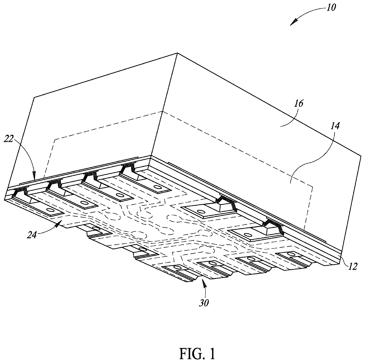
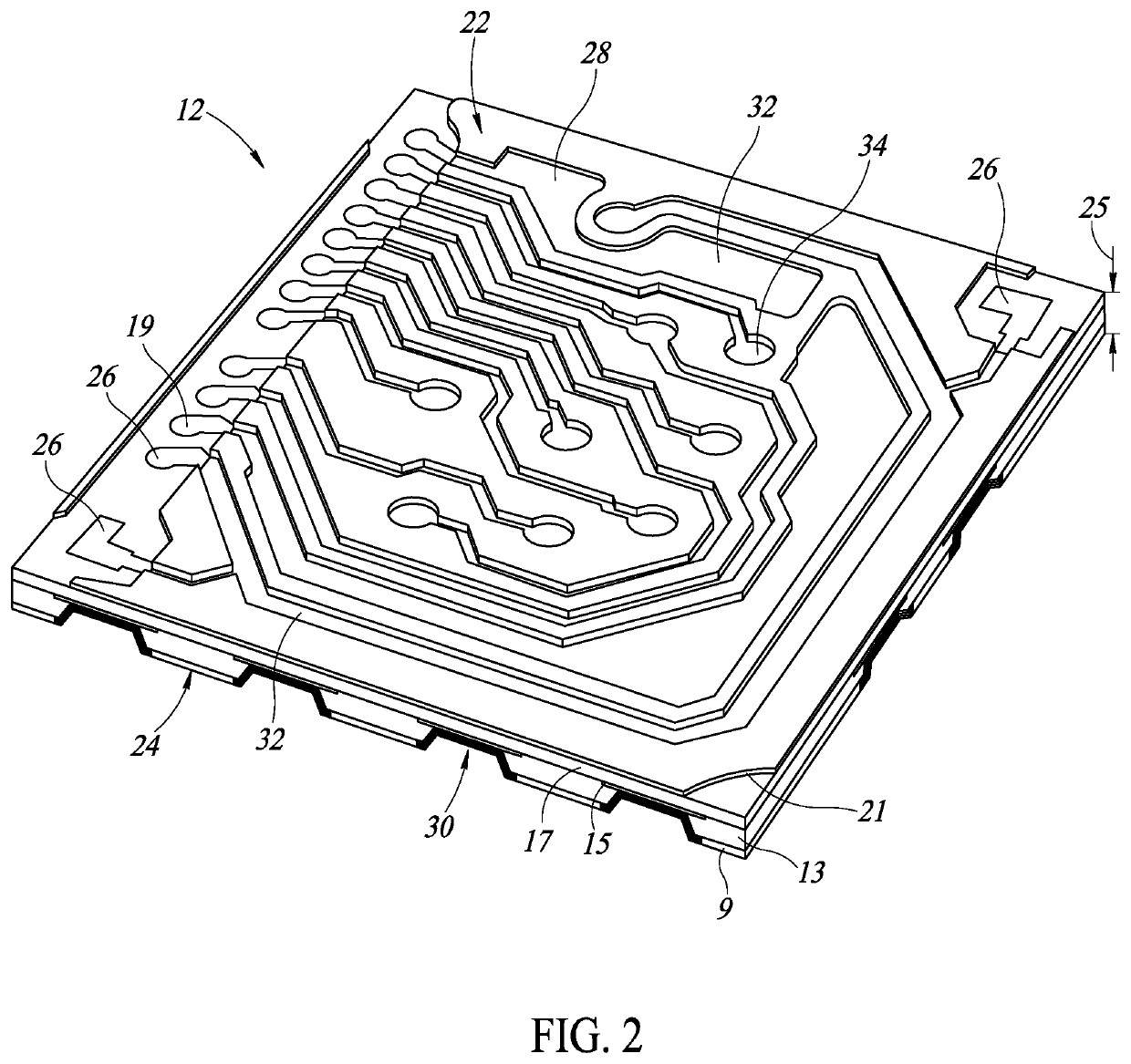
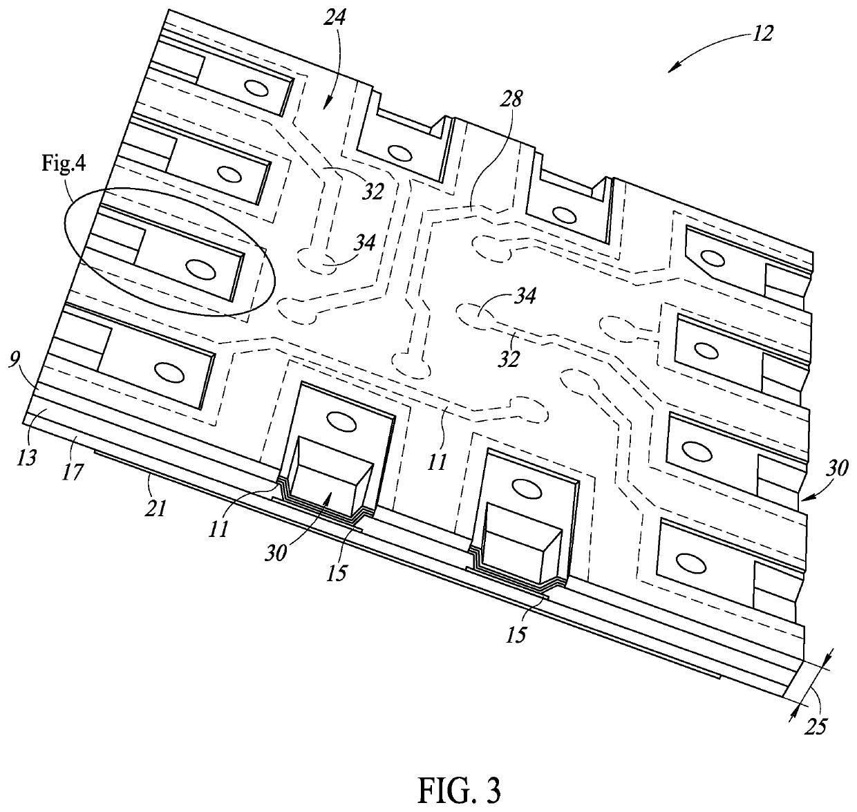
[0017]In the following description, certain specific details are set forth in order to provide a thorough understanding of various aspects of the disclosed subject matter. However, the disclosed subject matter may be practiced without these specific details. In some instances, well-known structures and methods of manufacturing electronic devices and semiconductor packages have not been described in detail to avoid obscuring the descriptions of other aspects of the present disclosure.

[0018]Unless the context requires otherwise, throughout the specification and claims that follow, the word “comprise” and variations thereof, such as “comprises” and “comprising,” are to be construed in an open, inclusive sense, that is, as “including, but not limited to.”

[0019]Reference throughout the specification to “one embodiment” or “an embodiment” means that a particular feature, structure, or characteristic described in connection with the embodiment is included in at least one embodiment. Thus, ...


PUM

PropertyMeasurementUnit
thicknessaaaaaaaaaa
thicknessaaaaaaaaaa
widthaaaaaaaaaa

Abstract

The present disclosure is directed to a semiconductor package including a substrate having a lower surface with a plurality of slot structures. The plurality of slot structures are multi-layer structures that encourage the formation of solder joints. The semiconductor package is desirable for high reliability applications in which each solder joint termination should be checked by visual systems to ensure a proper electrical connection has been made.

Description

BACKGROUNDTechnical Field[0001]The present disclosure is directed a semiconductor package for a semiconductor die.Description of the Related Art[0002]Semiconductor packages typically include a substrate, and a semiconductor die attached to the substrate. The substrate is electrically coupled to the semiconductor die, and includes various connection lines to carry electrical signals between the semiconductor die and, for example, a printed circuit board (PCB). Typically, the substrate is mounted on the PCB by soldering the substrate to the PCB. For example, semiconductor packages often include leads, sometimes referred to as lands, that are exposed on a bottom surface of the semiconductor package, and are electrically coupled to a PCB by soldering the leads to contact pads on the PCB.[0003]Subsequent to being soldered to a PCB, semiconductor packages are often inspected to ensure that proper electrical connections between the semiconductor package and the PCB have been made. For exam...

Claims


Application Information

Patent Timeline
Patent Type & Authority Patents(United States)
IPC IPC(8): H01L23/498H01L23/31
CPCH01L23/49838H01L23/3121H01L23/3157H01L23/49822H01L21/561H01L23/49805H01L23/49894
Inventor DEL SARTO, MARCOGRITTI, ALEXRECANATINI, PIERPAOLOBORG, MICHAEL
Owner STMICROELECTRONICS MALTA
Why Eureka
Try Eureka