Array substrate and method for preparing the same, display panel and display device

a technology of array substrate and substrate, applied in the field of array substrate and a method for preparing the same, a display panel and a display device, can solve problems such as uneven light emission of devices, and achieve the effects of simple process, low cost, and simple operation

Active Publication Date: 2022-04-26
BOE TECH GRP CO LTD
View PDF12 Cites 2 Cited by
  • Summary
  • Abstract
  • Description
  • Claims
  • Application Information

AI Technical Summary

Benefits of technology

[0003]Technology of inkjet printing polymer light-emitting diode (PLED) display has the advantages of simple operation, low cost, simple process, easy realization of large size, etc. With the continuous research and development of high-performance polymer materials and the further improvement of thin film preparation technology, PLED technology is expected to achieve rapid industrialization.

Problems solved by technology

Thus, the film formation in the pixel very uneven, thereby causing the device to emit light unevenly.

Method used


Image

  • Array substrate and method for preparing the same, display panel and display device
  • Array substrate and method for preparing the same, display panel and display device
  • Array substrate and method for preparing the same, display panel and display device

Examples


Embodiment Construction

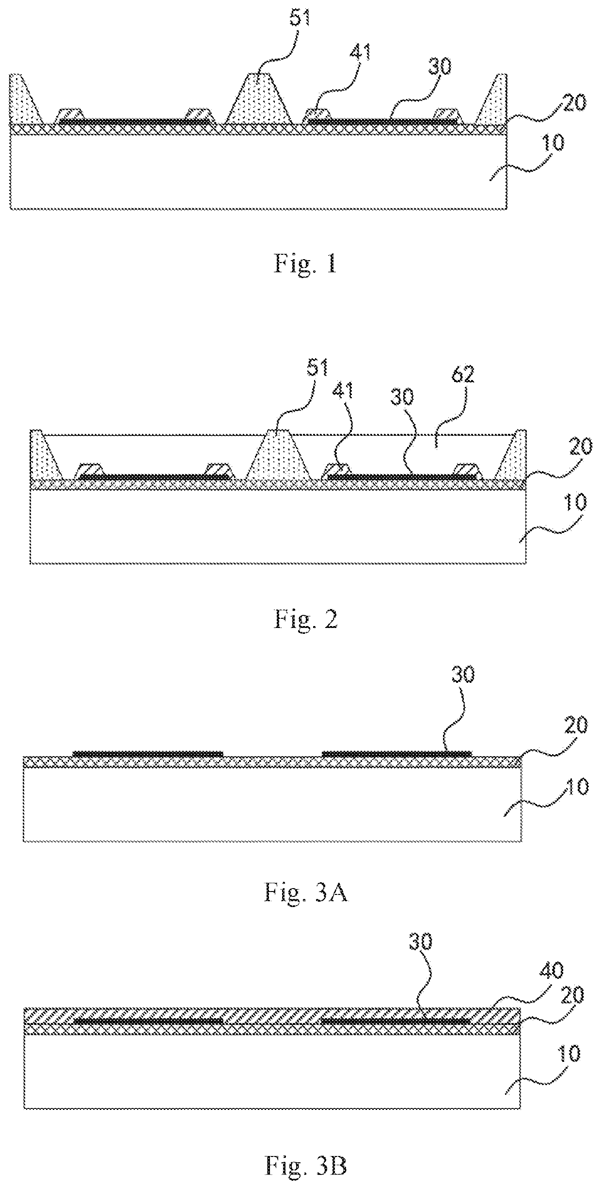
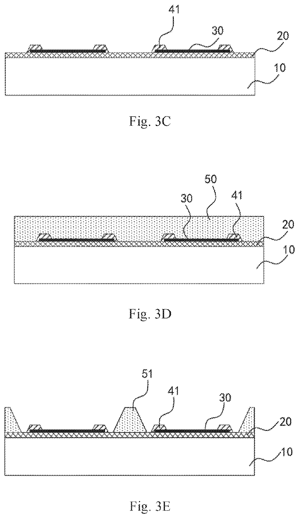
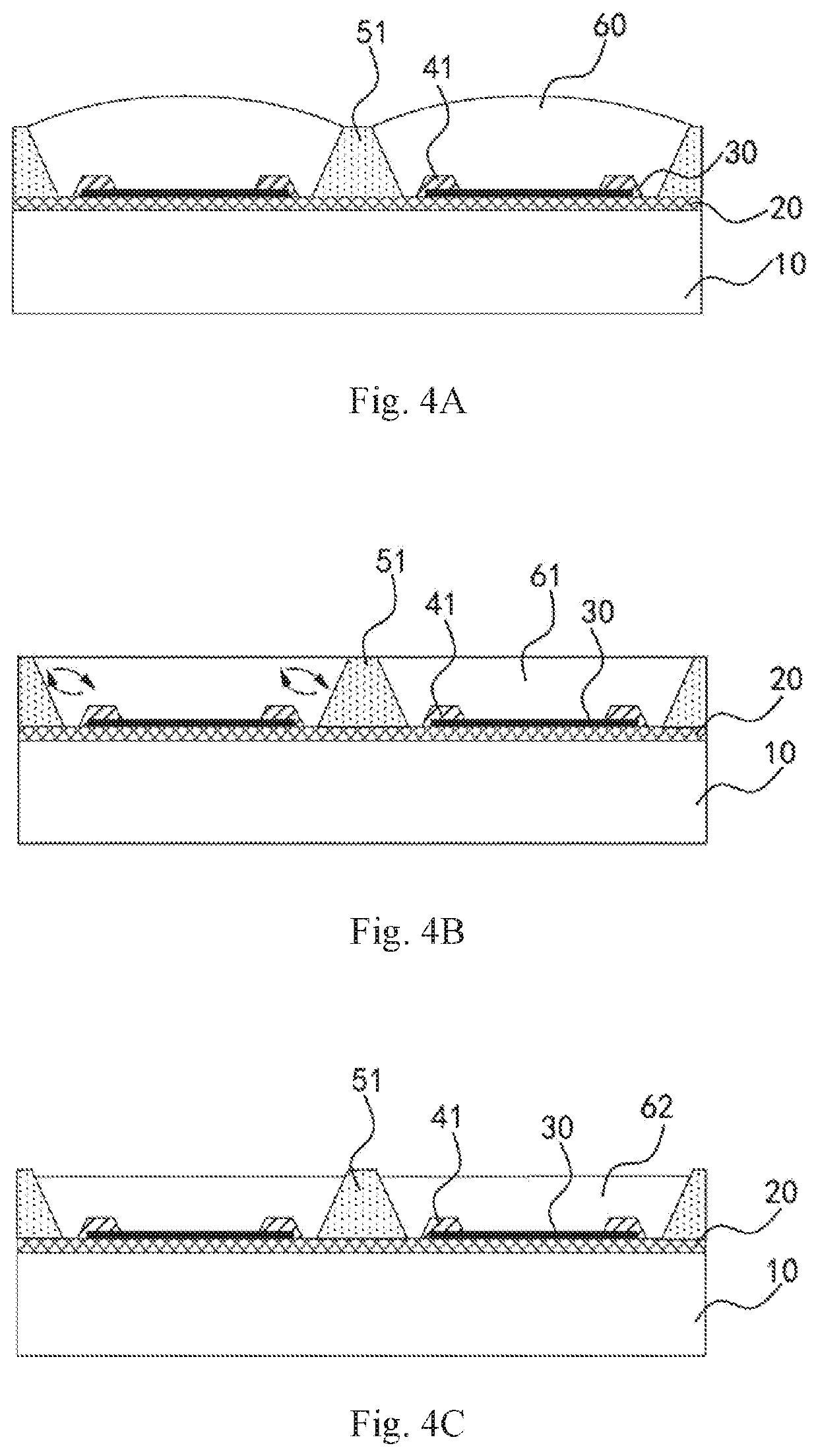
[0022]Exemplary embodiments will now be described in more details with reference to the drawings. However, the example embodiments can be implemented in various forms and should not be construed as being limited to the embodiments set forth herein; on the contrary, these embodiments are provided such that the present disclosure will be comprehensive and complete and the idea of the exemplary embodiments will be well understood by a person skilled in the art. In the drawings, the thicknesses of areas and layers are exaggerated for clarity. The similar reference numerals in the drawings denote the same or similar structures, and thus their detailed description will be omitted.

[0023]It should be noted that the terms “upper” and “lower” in this disclosure are merely relative concepts or refer to the normal use state of the product, and should not be considered as limitation.

[0024]Inkjet printing technology is to inject hole injection rials, and solutions of red, green, and blue light-em...


PUM

PropertyMeasurementUnit
widthaaaaaaaaaa
thicknessaaaaaaaaaa
thicknessaaaaaaaaaa

Abstract

The present disclosure provides an array substrate, including: a base substrate; a planarization layer formed on the base substrate; a plurality of pixel electrodes formed on the planarization layer; and a pixel definition layer including a first pixel definition layer and a second pixel definition layer, the first pixel definition layer covering a periphery of each pixel electrode and exposing a central area of each pixel electrode, the second pixel definition layer being formed on the planarization layer between adjacent pixel electrodes and having a plurality of openings defining each sub-pixel unit; a bottom of a dam portion of the second pixel definition layer and a bottom of a dam portion of the first pixel definition layer adjacent thereto are separated by a predetermined distance, and a thickness of the second pixel definition layer is greater than a thickness of the first pixel definition layer.

Description

CROSS-REFERENCE TO RELATED APPLICATIONS[0001]The present application is a U.S. national phase application of International Application No. PCT / CN2019 / 128735 filed on Dec. 26, 2019, which claims a priority to Chinese Patent Application No. 201910117700.1 filed on Feb. 15, 2019. The entire contents of each of the above-listed applications are hereby incorporated by reference for all purposes.TECHNICAL FIELD[0002]The present disclosure relates to the field of display technology, in particular, to an array substrate and a method for preparing the same, a display panel, and a display device.BACKGROUND AND SUMMARY[0003]Technology of inkjet printing polymer light-emitting diode (PLED) display has the advantages of simple operation, low cost, simple process, easy realization of large size, etc. With the continuous research and development of high-performance polymer materials and the further improvement of thin film preparation technology, PLED technology is expected to achieve rapid indust...

Claims


Application Information

Patent Timeline
Patent Type & Authority Patents(United States)
IPC IPC(8): H01L27/32H01L51/00H01L51/56
CPCH01L27/3246H01L51/0005H01L51/56H01L2251/558H10K59/122H10K71/135H10K59/1201H10K71/00H10K2102/351
Inventor CUI, YING
Owner BOE TECH GRP CO LTD
Why Eureka
Try Eureka