
Scalable tester for testing multiple devices under test

a tester and test device technology, applied in the direction of electronic circuit testing, measurement devices, instruments, etc., can solve the problems of high cost of testers, limited test boards, complex test boards,

Active Publication Date: 2022-05-03
GAOIRAN ALBERT
View PDF8 Cites 8 Cited by
  • Summary
  • Abstract
  • Description
  • Claims
  • Application Information

AI Technical Summary

Benefits of technology

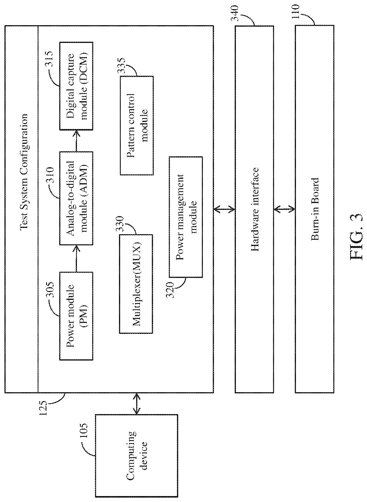
The test system configuration includes various modules that are used as building blocks to design testing for a given DUT (device under test). These modules can be used repeatedly and can be customized to provide the tests desired for a given DUT. The system is scalable in that it can be used to test any DUT having any number of channels or pins without the need for additional modules or testers. The technical effect of this is that it allows for efficient and customizable testing of multiple DUTs with minimal additional resources.

Problems solved by technology

However, such testing boards are complex and bulky.
Test boards are also limited to testing a set number of DUTs based on the number of available sockets, as well as a given number of channels per DUT based upon the available channels on the test board, the fixed number of resources available to use such channels, and the software available to control such resources.
This limits the use of the tester to DUTs of one particular dimension and hence makes the tester expensive.
Further, the tester requires manual intervention.
However, existing systems for checking test setups also utilize and are limited by a fixed number of resources.
Increasing complexity of integrated circuits and semiconductor devices has made their testing more challenging with existing testers.
For example, testing complex integrated circuits requires high current and low voltage.
Hence, power supplies that provide the high current and the low voltage incur additional costs for testing, resulting in testing costs being a higher percentage of the total manufacture cost of the integrated circuit.
For example, due to increasing complexity of semiconductor devices, manufacturers are forced to buy new equipment having the required test resources, which requires training to implement any reliability tests, increasing time-to-market for the device.

Method used


Image

  • Scalable tester for testing multiple devices under test
  • Scalable tester for testing multiple devices under test
  • Scalable tester for testing multiple devices under test

Examples


Embodiment Construction

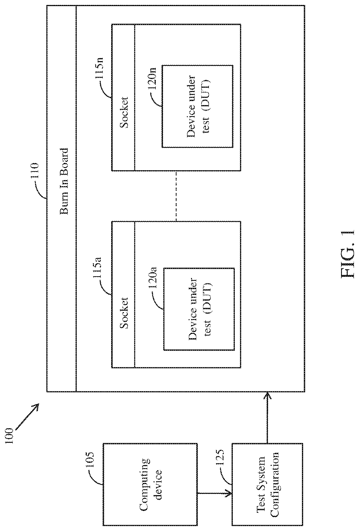
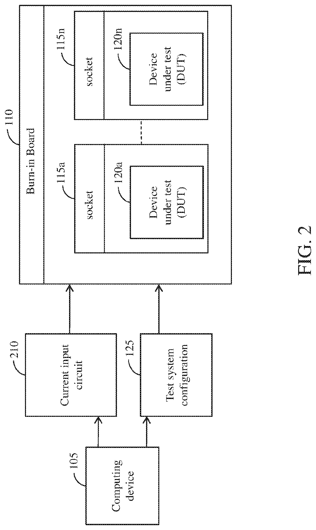
[0020]The present invention is more fully described below with reference to the accompanying Figures. While the invention will be described in conjunction with particular embodiments, it should be understood that the invention includes alternatives, modifications, and equivalents. Accordingly, the following description is exemplary in that several embodiments are described (e.g., by use of the terms “preferably,”“for example,” or “in one embodiment”), but this description should not be viewed as limiting or as setting forth the only embodiments of the invention, as the invention encompasses other embodiments not specifically recited in this description. Further, the use of the terms “invention,”“present invention,”“embodiment,” and similar terms throughout this description are used broadly and are not intended to mean that the invention requires, or is limited to, any particular aspect being described or that such description is the only manner in which the invention may be made or ...


PUM


Abstract

Various embodiments of the invention provide a system and a method for testing one or more devices under test (DUTs) and for checking one or more test setups. Each of the one or more test setups includes a test board having several sockets for receipt of a DUT. A custom hardware interface is used to electrically connect the test board, such as a burn-in board with a test system configuration having multiple modules that can be configured using a computer device and related software to provide customized testing of the DUTs. The system is scalable to accommodate any DUT having any number of channels and to provide customized testing. Results of the testing are sent to the computing device.

Description

CROSS-REFERENCE TO RELATED APPLICATIONS[0001]This application is a continuation of U.S. patent application Ser. No. 15 / 411,689 filed Jan. 20, 2017, which claims the benefit of provisional Application No. 62 / 281,733, filed Jan. 22, 2016. The entireties of the foregoing applications are incorporated by reference herein.BACKGROUND OF THE INVENTIONField of the Invention[0002]The invention in its various embodiments relates generally to testing devices under test or DUTs. In particular, the invention in its various embodiments relates to a system and a method for testing DUTs that is customizable for any DUT and that is scalable to the number of pins on the DUT, particularly for DUT testing using a burn-in board.Description of Related Art[0003]Devices, for example, integrated circuit devices, need to be tested before marketing. The devices, while undergoing testing, are referred to as “devices under test” (DUTs). The DUTs are tested by connecting the DUTs with a test board. Various testi...

Claims


Application Information

Patent Timeline
Patent Type & Authority Patents(United States)
IPC IPC(8): G01R31/28G01R1/04
CPCG01R31/2849G01R1/0408G01R31/31907
Inventor GAOIRAN, ALBERT
Owner GAOIRAN ALBERT
Learn More