Method of making memory cells, high voltage devices and logic devices on a substrate with silicide on conductive blocks
a technology of memory cells and conductive blocks, applied in the field of semiconductor devices, can solve problems such as adversely affecting the concurrent fabrication of logic devices
- Summary
- Abstract
- Description
- Claims
- Application Information
AI Technical Summary
Benefits of technology
Problems solved by technology
Method used
Image


Examples
Embodiment Construction
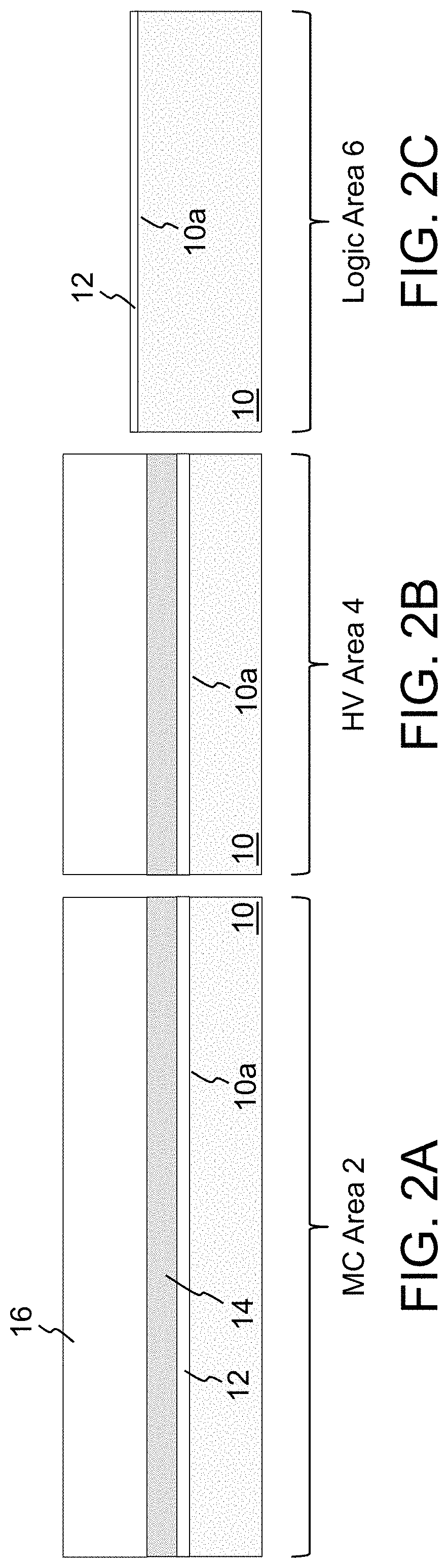
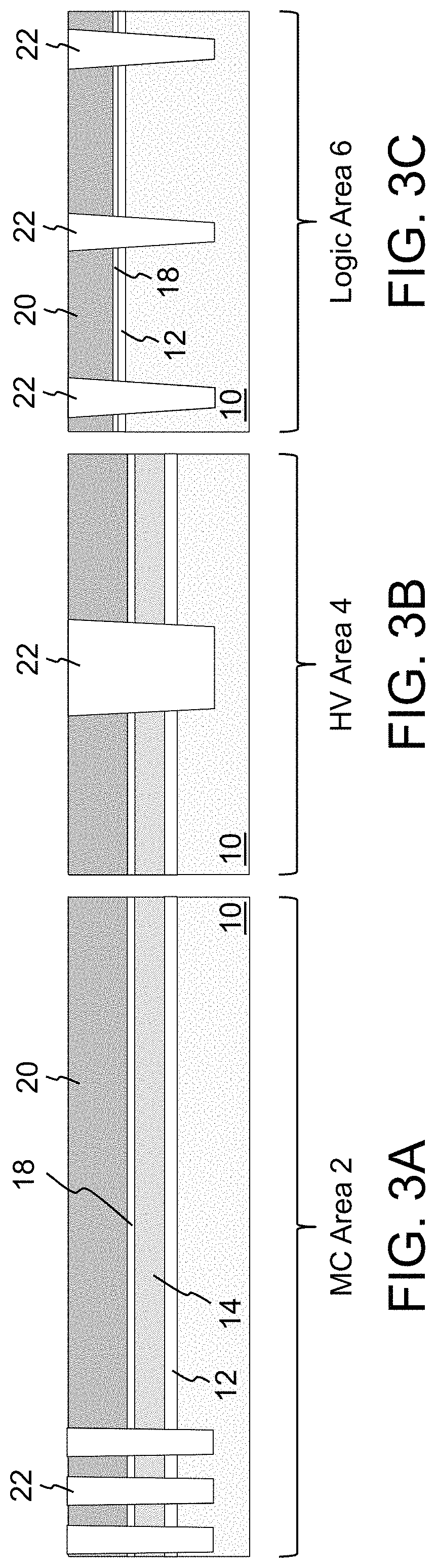
[0039]The present invention is a process of forming a semiconductor device by simultaneously forming memory cells, low voltage logic devices and high voltage logic devices on the same semiconductor substrate. The process described below involves forming memory cells in one or more memory cell areas (also referred to as first or MC areas) 2 of the substrate 10, high voltage logic devices in one or more high voltage logic device areas (also referred to as second or HV areas) 4 of the substrate 10, and low voltage logic devices in one or more low voltage logic device areas (also referred to a third or logic areas) 6 of the substrate 10. The process is described with respect to forming a pair of memory cells in the MC area 2, a high voltage logic device in the HV area 4, and a lower voltage logic device in the logic area 6, simultaneously. However, multiple such devices in each area are simultaneously formed. Substrate 10 is a substrate of semiconductor material (e.g., silicon).
[0040]Re...
PUM
| Property | Measurement | Unit |
|---|---|---|
| area | aaaaa | aaaaa |
| conductive | aaaaa | aaaaa |
| semiconductor | aaaaa | aaaaa |
Abstract
Description
Claims
Application Information