Testing circuitry and methods for analog neural memory in artificial neural network

a neural network and analog neural network technology, applied in the field of testing circuitry and methods for analog neural network analog neural network, can solve the problems of cmos-implemented synapses being too bulky, lack of hardware technology for performance information processing, and mediocre energy efficiency

Active Publication Date: 2022-07-19
SILICON STORAGE TECHNOLOGY
View PDF16 Cites 0 Cited by
  • Summary
  • Abstract
  • Description
  • Claims
  • Application Information

AI Technical Summary

Problems solved by technology

One of the major challenges in the development of artificial neural networks for high-performance information processing is a lack of adequate hardware technology.
However, in addition to high cost, these approaches also suffer from mediocre energy efficiency as compared to biological networks, which consume much less energy primarily because they perform low-precision analog computation.
CMOS analog circuits have been used for artificial neural networks, but most CMOS-implemented synapses have been too bulky given the high number of neurons and synapses required.

Method used


Image

  • Testing circuitry and methods for analog neural memory in artificial neural network
  • Testing circuitry and methods for analog neural memory in artificial neural network
  • Testing circuitry and methods for analog neural memory in artificial neural network

Examples


Embodiment Construction

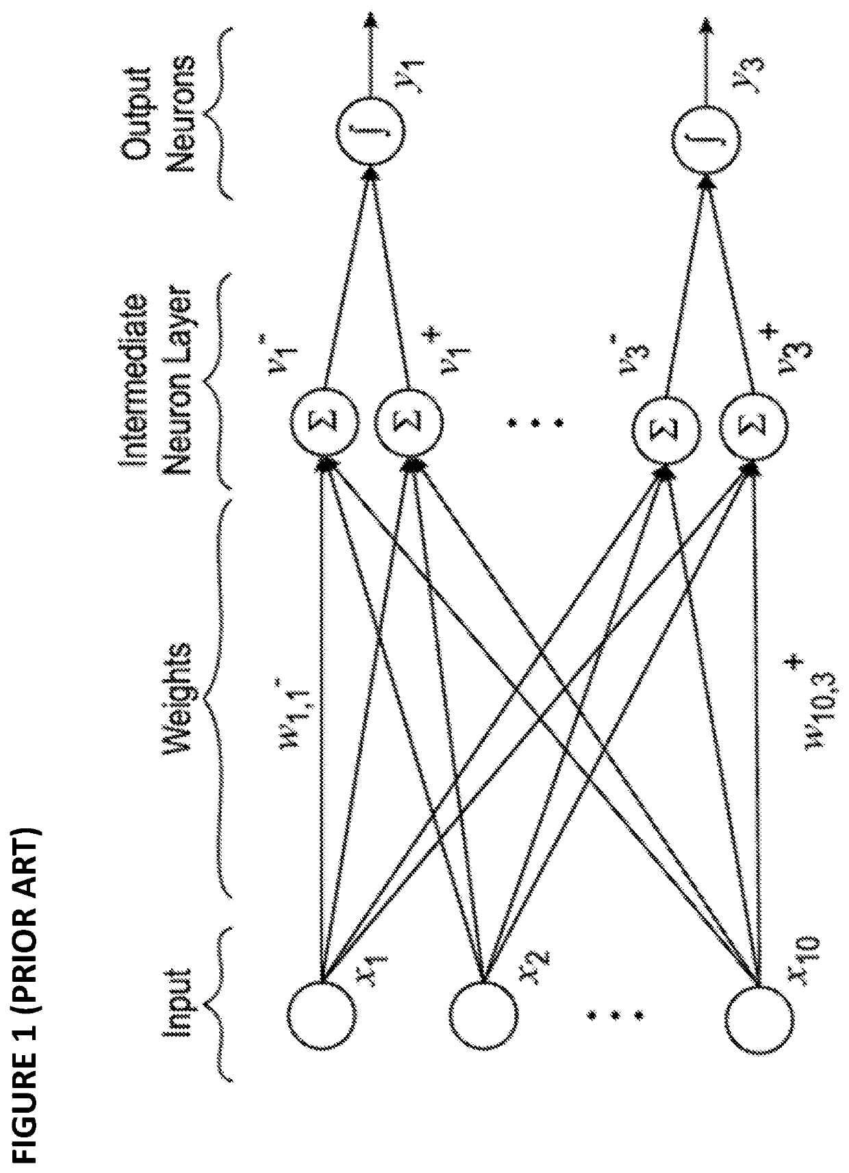
[0069]The artificial neural networks of the present invention utilize a combination of CMOS technology and non-volatile memory arrays.

[0070]Non-Volatile Memory Cells

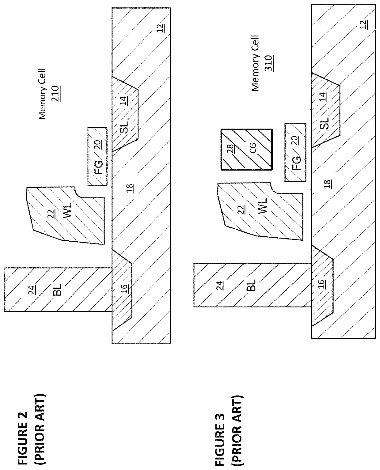
[0071]Digital non-volatile memories are well known. For example, U.S. Pat. No. 5,029,130 (“the '130 patent”), which is incorporated herein by reference, discloses an array of split gate non-volatile memory cells, which are a type of flash memory cells. Such a memory cell 210 is shown in FIG. 2. Each memory cell 210 includes source region 14 and drain region 16 formed in semiconductor substrate 12, with channel region 18 there between. Floating gate 20 is formed over and insulated from (and controls the conductivity of) a first portion of the channel region 18, and over a portion of the source region 14. Word line terminal 22 (which is typically coupled to a word line) has a first portion that is disposed over and insulated from (and controls the conductivity of) a second portion of the channel region 18, and a second por...


PUM


Abstract

Testing circuitry and methods are disclosed for use with analog neural memory in deep learning artificial neural networks. The analog neural memory comprises one or more arrays of non-volatile memory cells. The testing circuitry and methods can be utilized during sort tests, qualification tests, and other tests to verify programming operations of one or more cells.

Description

PRIORITY CLAIM[0001]This application claims priority from U.S. Provisional Patent Application No. 62 / 876,515, filed on Jul. 19, 2019, and titled, “Testing Circuitry and Methods for Analog Neural Memory in Artificial Neural Network,” which is incorporated by reference herein.FIELD OF THE INVENTION[0002]Testing circuitry and methods are disclosed for use with analog neural memory in deep learning artificial neural networks. The analog neural memory comprises one or more arrays of non-volatile flash memory cells.BACKGROUND OF THE INVENTION[0003]Artificial neural networks mimic biological neural networks (the central nervous systems of animals, in particular the brain) and are used to estimate or approximate functions that can depend on a large number of inputs and are generally unknown. Artificial neural networks generally include layers of interconnected “neurons” which exchange messages between each other.[0004]FIG. 1 illustrates an artificial neural network, where the circles repres...

Claims


Application Information

Patent Timeline
Patent Type & Authority Patents(United States)
IPC IPC(8): G11C16/34G11C16/10G06N3/063G06F3/06G06N3/08G11C16/26G11C29/10
CPCG11C16/3459G06F3/0688G06N3/063G06N3/08G11C16/10G11C16/26G11C16/3436G11C29/10G11C11/54G11C16/0425G11C2029/5006G11C2029/1204G11C29/50G11C2029/2602G06N3/065G06N3/048
Inventor TRAN, HIEU VANVU, THUANTRINH, STEPHENHONG, STANLEYLY, ANHLEMKE, STEVENNGUYEN, NHATIWARI, VIPINDO, NHAN
Owner SILICON STORAGE TECHNOLOGY
Why Eureka
Try Eureka