Circuit simulation device for predicting the dispersion of circuit characteristics and the electric characteristics

a circuit simulation and electric characteristic technology, applied in the field of circuit simulation, can solve the problems of inability to accurately predict parameters given by adverse affection, inability to accurately predict parameters when the gate length and gate width change, and inability to accurately predict circuit characteristics

Inactive Publication Date: 2001-07-05
KK TOSHIBA
View PDF1 Cites 9 Cited by
  • Summary
  • Abstract
  • Description
  • Claims
  • Application Information

AI Technical Summary

Benefits of technology

[0027] In addition, it is still another object of the present invention to provide a computer readable recording medium in which a circuit simulation program for considerably improving the yield of a circuit manufacturing process is stored.
[0028] Furthermore, it is still another object of the present invention to provide a circuit manufacturing method for considerably improving the yield of a circuit manufacturing process.
[0029] For the technical problems described above, the present inventors correctly reflect the magnitude of the dispersions of gate lengths and gate widths on a specific circuit parameter to extract another circuit parameter, so that the influence of the dispersions of the gate lengths and the gate widths is prevented from adversely affecting circuit parameters except for the specific circuit parameter. For this reason, the circuit parameters can be correctly extracted, and circuit characteristics can be accurately predicted. As a result, the present inventors thought that manufacturing conditions for a circuit having desired circuit characteristics could be correctly determined to make it possible to perform a semiconductor manufacturing process at a high yield.
[0031] According to the present invention, since actual gate lengths and actual gate widths are used in extraction of circuit parameters, the circuit parameters can be extracted at a high accuracy.
[0032] Furthermore, according to the present invention, when circuit characteristics are to be analyzed, dispersion can be given to gate lengths and gate widths. For this reason, the dispersion of circuit characteristics can be correctly evaluated, and the magnitude of the dispersion can be correctly predicted.

Problems solved by technology

However, the conventional circuit manufacturing process has the following technical problem to be solved.
For this reason, the differences (Lerr=Lactual-L0, Werr=Wactual-W0) between the gate lengths (gate widths W) adversely affect the other circuit parameters.
In addition, since the adverse affection changes depending on an extraction strategy of the circuit parameters, parameters which the adverse affection are given cannot be predicted at all.
More specifically, in the conventional circuit manufacturing process, since the circuit parameters which are adversely affected by the influence of the errors of the gate lengths and the gate widths cannot be physically and correctly extracted, the circuit characteristics when the gate lengths and the gate widths change cannot be correctly predicted.
As a result, the yield of the circuit manufacturing process cannot be improved.
A physically correct value cannot be obtained.
Second, in the conventional circuit manufacturing process, unlike in the second dispersion predicting method, information related to variation in the gate length L (gate width W) is not transmitted to the circuit simulation.
As a result, the yield of the circuit manufacturing process cannot be improved.

Method used


Image

  • Circuit simulation device for predicting the dispersion of circuit characteristics and the electric characteristics
  • Circuit simulation device for predicting the dispersion of circuit characteristics and the electric characteristics
  • Circuit simulation device for predicting the dispersion of circuit characteristics and the electric characteristics

Examples


first embodiment

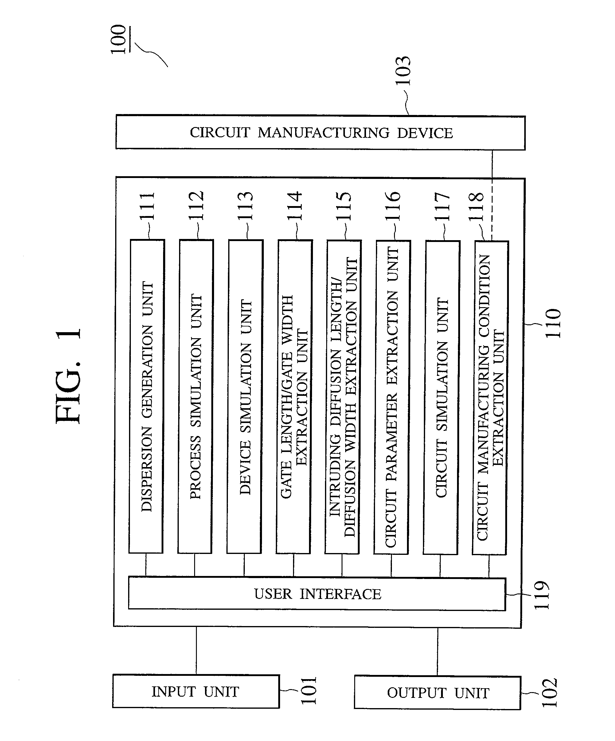
[0042] First, the configuration of a circuit manufacturing system according to the present invention will be described below.

[0043] FIG. 1 is a block diagram showing the configuration of a circuit manufacturing system according to the first embodiment of the present invention.

[0044] A circuit manufacturing system 100 according to the first embodiment of the present invention is constituted by, as shown in FIG. 1, a circuit manufacturing condition extraction device 110 for predicting the dispersion of circuit characteristics caused by variation in a manufacturing process of a semiconductor element and for determining manufacturing conditions of a circuit with reference to the result of the prediction, and a circuit manufacturing device 103 for manufacturing a circuit on the basis of the circuit manufacturing conditions determined by the circuit manufacturing condition extraction device 110.

[0045] The circuit manufacturing condition extraction device 110 comprises a dispersion generat...

second embodiment

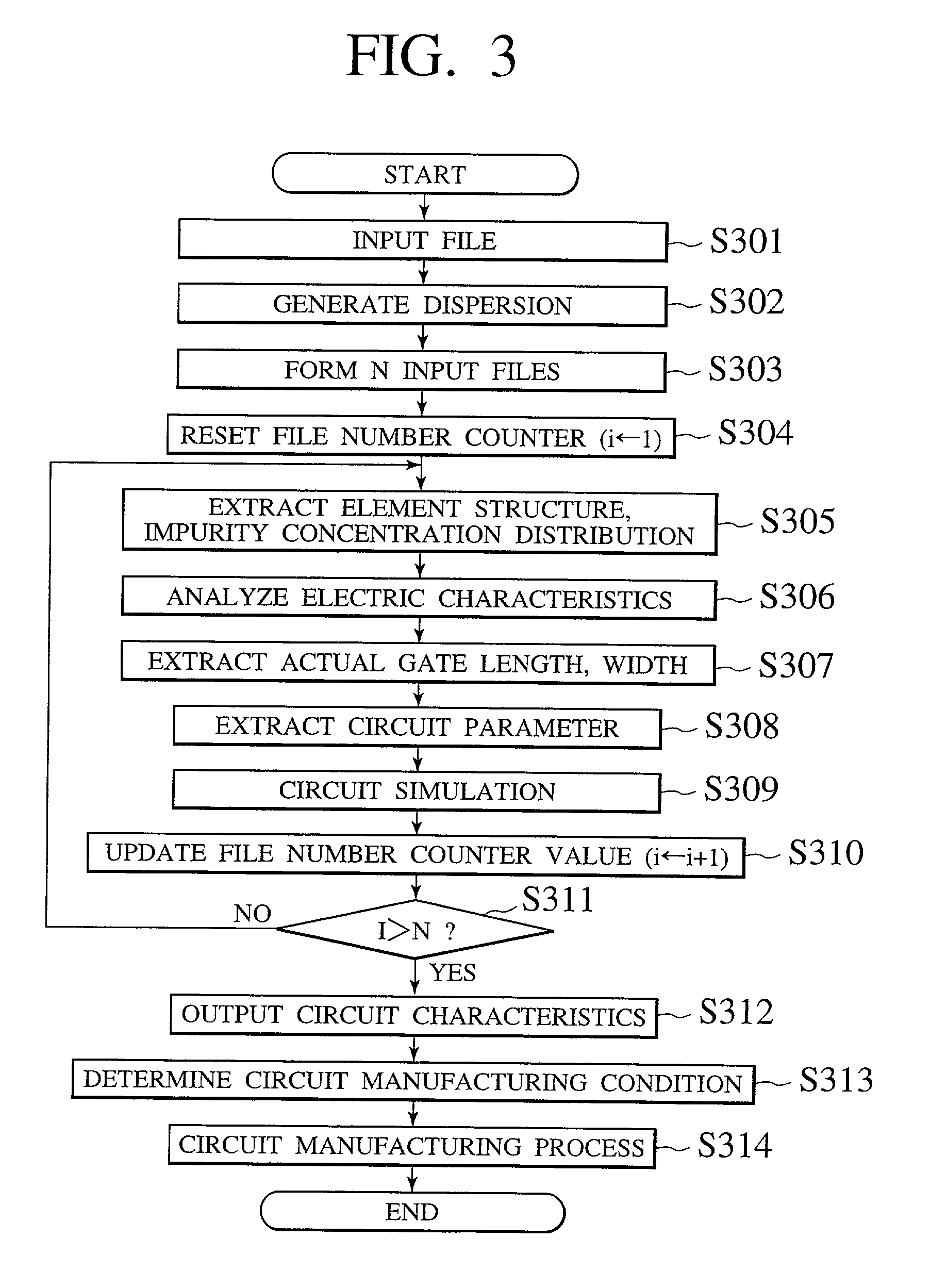
[0070] A circuit manufacturing system and an operation (circuit manufacturing method) according to the second embodiment of the present invention will be described below. Since the configuration of a circuit manufacturing system according to the second embodiment of the present invention is the same as that of the first embodiment, a description thereof will be omitted. The circuit manufacturing method according to the second embodiment of the present invention will be described below.

[0071] FIG. 3 is a flow chart showing the circuit manufacturing method according to the second embodiment of the present invention.

[0072] A circuit manufacturing process using the circuit manufacturing method according to the second embodiment of the present invention will be executed by the following steps.

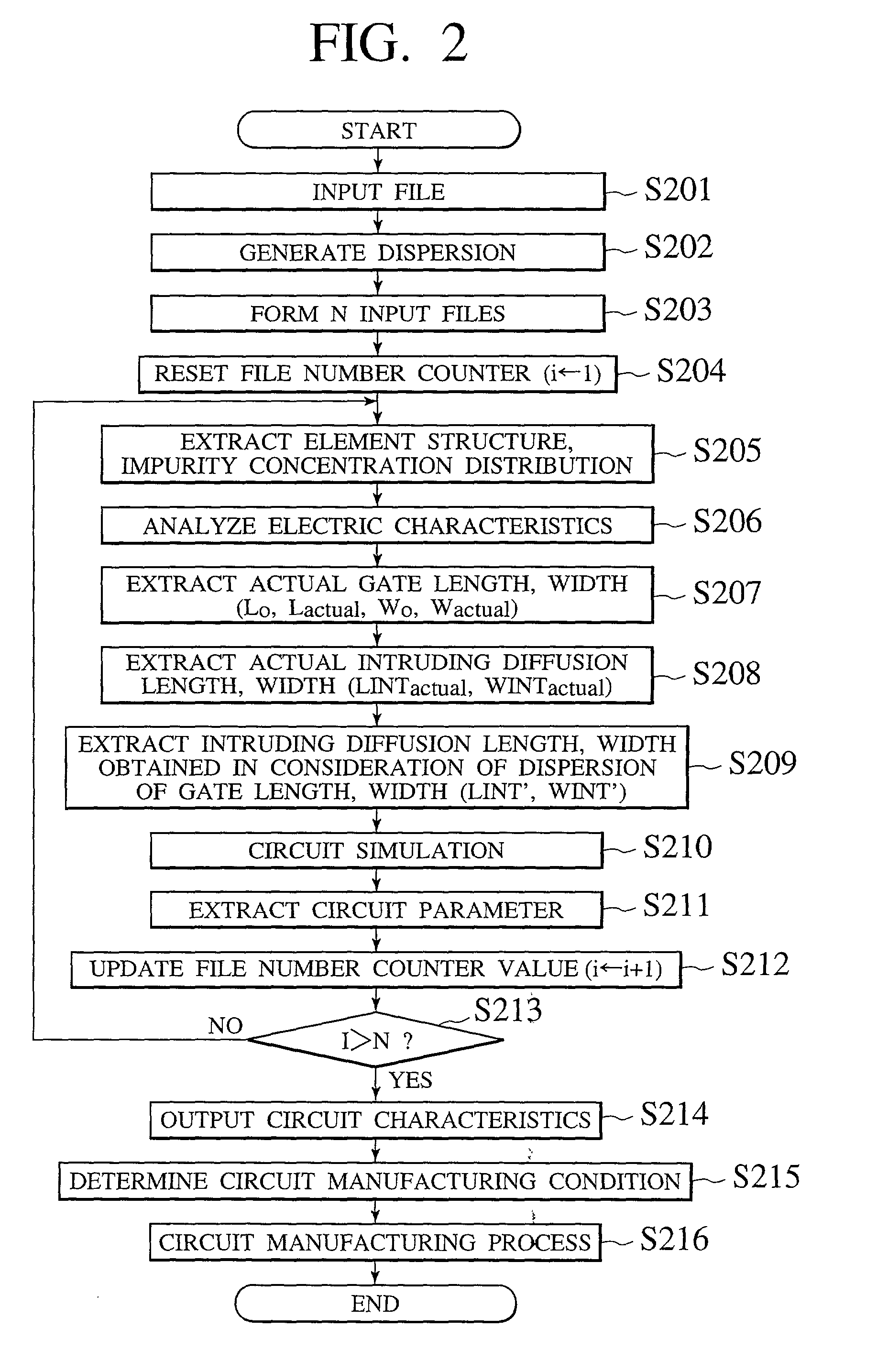
[0073] (1) Process conditions in the step of manufacturing MOSFETs and a file for process simulation in which a gate length L0 and a gate width W0 of a mask (design value) are described are input (f...


PUM


Abstract

In the disclosed invention, the influence of the dispersions of the gate lengths and the gate widths is prevented from adversely affecting circuit parameters except for the specific circuit parameter. According to this invention, the circuit parameters can be correctly extracted, and circuit characteristics can be accurately predicted.

Description

[0001] The subject application is related to subject matter disclosed in the Japanese Patent Application No.Hei11-375842 filed in Dec. 28, 1999 in Japan, to which the subject application claims priority under the Paris Convention and which is incorporated by reference herein.[0002] 1. Field of the Invention[0003] The present invention relates to a circuit simulation device for, by using pieces of information related to the element structures and electric characteristics of a plurality of semiconductor elements, predicting the dispersion of circuit characteristics caused by differences of the element structures and the electric characteristics from design values, a circuit simulation method, a circuit simulation program product, and a circuit manufacturing method for, by using pieces of information related to the element structures and electric characteristics of a plurality of semiconductor elements, predicting the dispersion of circuit characteristics caused by differences of the e...

Claims


Application Information

Patent Timeline
Patent Type & Authority Applications(United States)
IPC IPC(8): G06F17/50H01L21/822H01L21/66H01L21/82H01L27/04
CPCH01L22/20
Inventor WAKITA, NAOKIYAMAGUCHI, TETSUYA
Owner KK TOSHIBA
Why Eureka
Try Eureka