Clock control circuit and clock control method

a clock control and clock technology, applied in the direction of pulse technique, oscillation generator, generating/distributing signals, etc., to achieve the effect of reducing phase error to a major degr

Inactive Publication Date: 2001-10-04
RENESAS ELECTRONICS CORP
View PDF0 Cites 102 Cited by
  • Summary
  • Abstract
  • Description
  • Claims
  • Application Information

AI Technical Summary

Benefits of technology

0013] Accordingly, an object of the present invention, in one aspect, is to provide a clock control circuit and method as well as a semiconductor integrated circuit device in which center-frequency fluctuation caused when a PLL is used and ji...

Problems solved by technology

The clock control circuits according to the prior art...

Method used


Image

  • Clock control circuit and clock control method
  • Clock control circuit and clock control method
  • Clock control circuit and clock control method

Examples


second embodiment

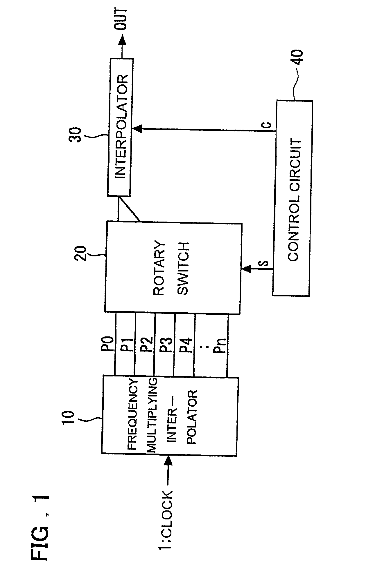
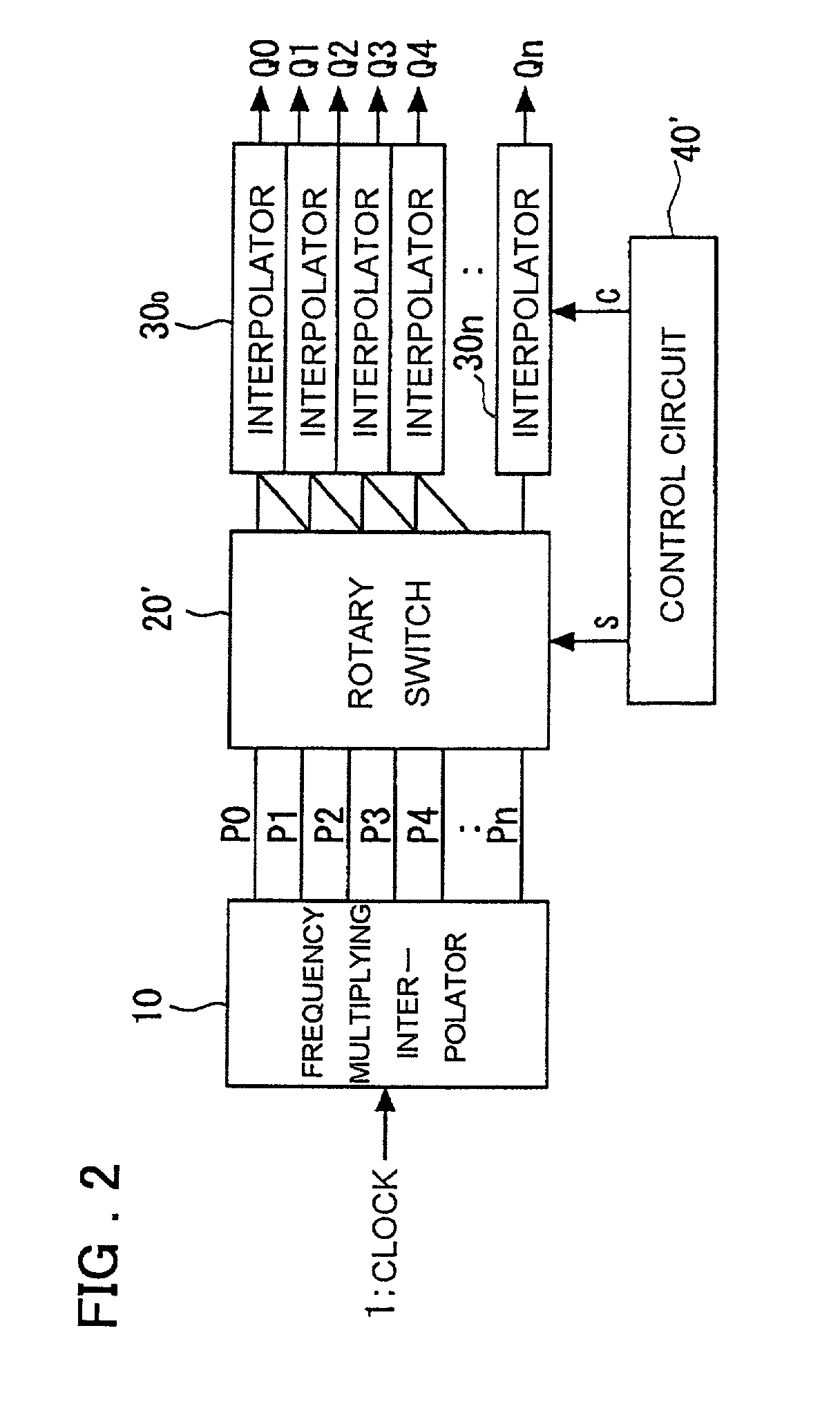
[0134] FIG. 2 is a block diagram illustrating the structure of the present invention;

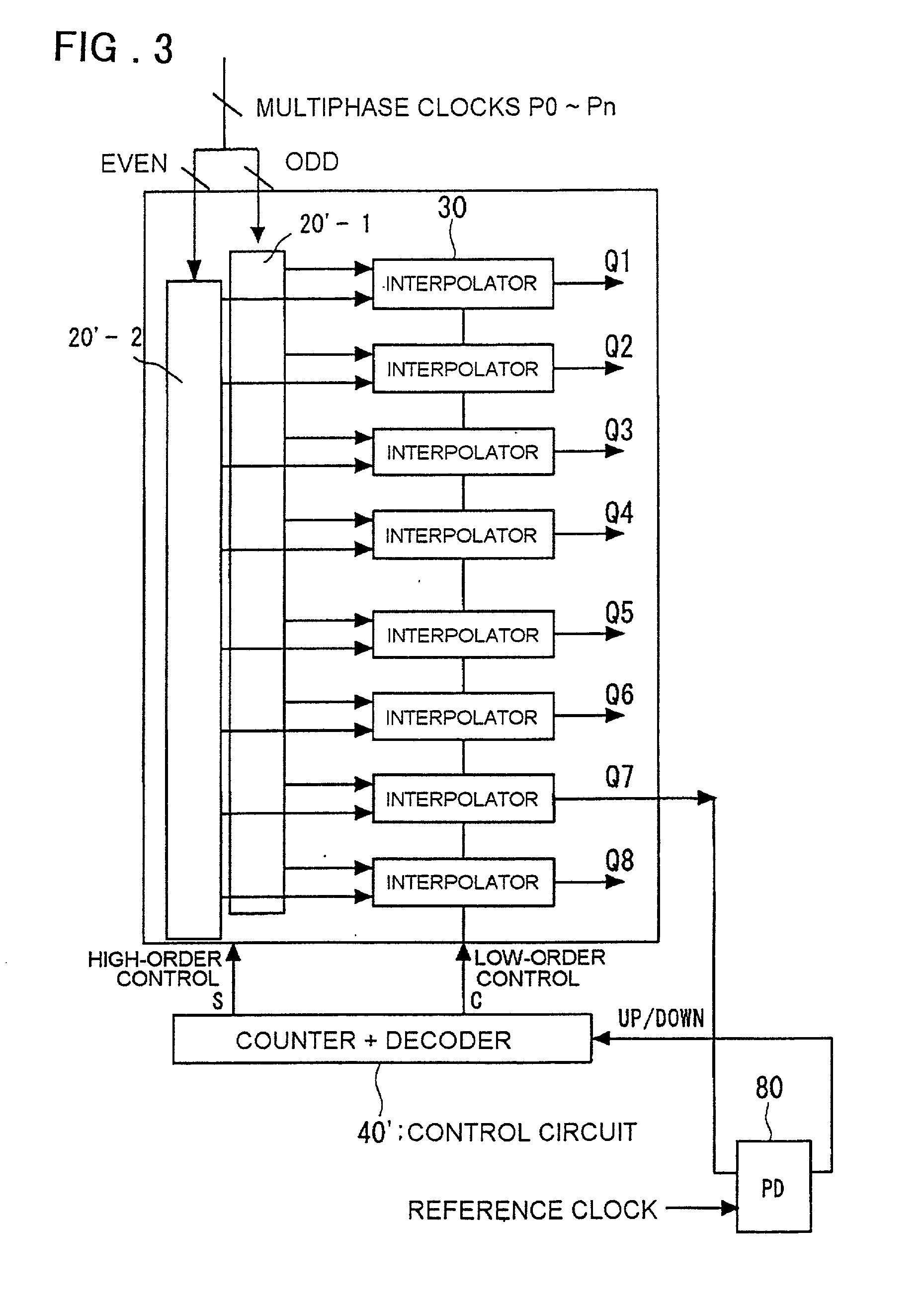
[0135] FIG. 3 is a block diagram illustrating the structure of the second embodiment of the present invention;

[0136] FIG. 4 is a block diagram illustrating the structure of a frequency multiplying interpolator according to an embodiment of the present invention;

[0137] FIG. 5 is a block diagram illustrating the structure of a frequency multiplying interpolator according to an embodiment of the present invention;

[0138] FIGS. 6(a), (b) and (c) are diagrams illustrating the structure of a 4-phase-clock frequency multiplying circuit according to an embodiment of the present invention;

[0139] FIG. 7 is a diagram showing the timing waveforms of the 4-phase-clock frequency multiplying circuit according to the embodiment of the present invention shown in FIG. 6;

[0140] FIGS. 8(a) and (b) diagrams showing the structures of timing-difference dividing circuits of the 4-phase-clock frequency multiplying circuit ac...

third embodiment

[0147] FIG. 15 is a block diagram illustrating the structure of the present invention;

[0148] FIG. 16 is a block diagram illustrating the structures of a switch and interpolator according to the third embodiment of the present invention;

[0149] FIG. 17 is a diagram showing an example of the layout of a 16-step interpolator according to an embodiment of the present invention;

fourth embodiment

[0150] FIG. 18 is a block diagram illustrating the present invention;


PUM


Abstract

A clock control circuit which includes a frequency multiplying interpolator for generating and outputting multiphase clocks by frequency multiplying an input clock; a switch for outputting two of the multiphase clocks input thereto from the frequency multiplying interpolator; a fine adjusting interpolator, to which the two outputs from the switch are applied, for outputting a signal obtained by internally dividing the phase difference between the two outputs; and a control circuit for controlling the switching of the switch and varying the internal-division ratio of the fine adjusting interpolator.

Description

[0001] This invention relates to clock control technology and, more particularly, to a clock control circuit and method using an interpolator for frequency multiplication.[0002] In order to deal with an increase in the scale of circuitry that can be integrated on a single chip and in order to handle higher operating frequencies, semiconductor integrated circuits which include a synchronizing circuit that operates upon being supplied with a clock are provided with a clock control circuit for controlling phase and frequency of clocks externally and internally of the chip.[0003] A PLL (Phase-Locked Loop) or a DLL (Delay-Locked Loop) is used conventionally as such a clock control circuit. In semiconductor circuits having system-scale circuitry on a single chip such as an LSI chip (referred to also as a "system on silicon"), it is now necessary to provide a clock control circuit for phase and frequency control for each macroblock within the chip, by way of example.[0004] In addition to u...

Claims


Application Information

Patent Timeline
IPC IPC(8): H03K5/00G06F1/06H03L7/00H03L7/081
CPCH03K5/131H03K5/135H03K5/156H03K2005/00052H03L7/07H03L7/0805H03L7/0814H03L7/0816H03L7/00
Inventor SAEKI, TAKANORI
Owner RENESAS ELECTRONICS CORP
Why Eureka
Try Eureka