

Block symmetrization in a field programmable gate array
a field programmable gate array and block symmetrization technology, applied in the direction of instruments, computation using denominational number representation, pulse technique, etc., can solve the problem that the reprogrammable sram bit cannot be provided to connect routing resources, and the place and route of nets in an sram based fpga is difficul
- Summary
- Abstract
- Description
- Claims
- Application Information
AI Technical Summary
Benefits of technology
Problems solved by technology
Method used
Image

Examples
Embodiment Construction
[0020] Those of ordinary skill in the art will realize that the following description of the present invention is illustrative only and not in any way limiting. Other embodiments of the invention will readily suggest themselves to such skilled persons.
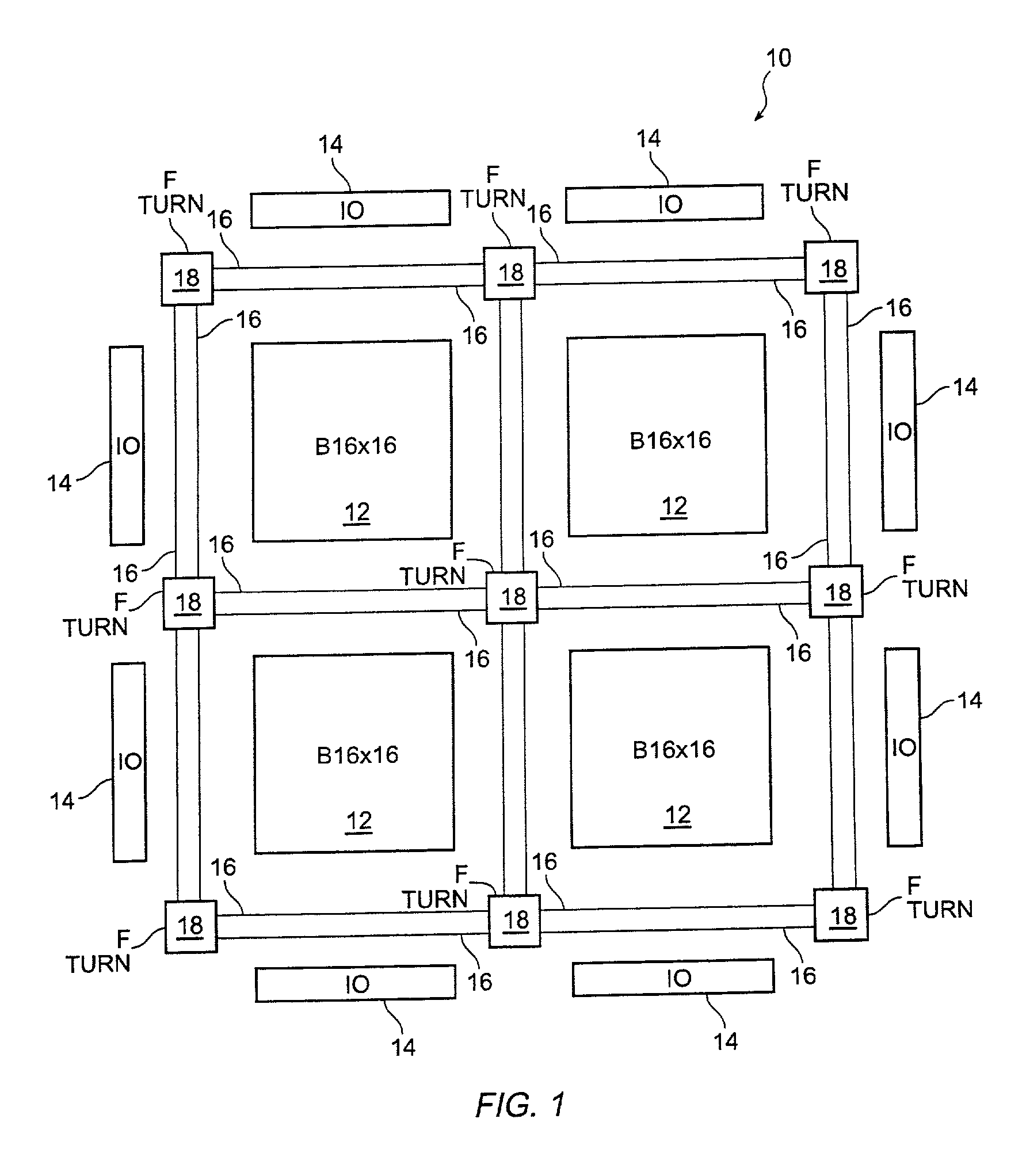
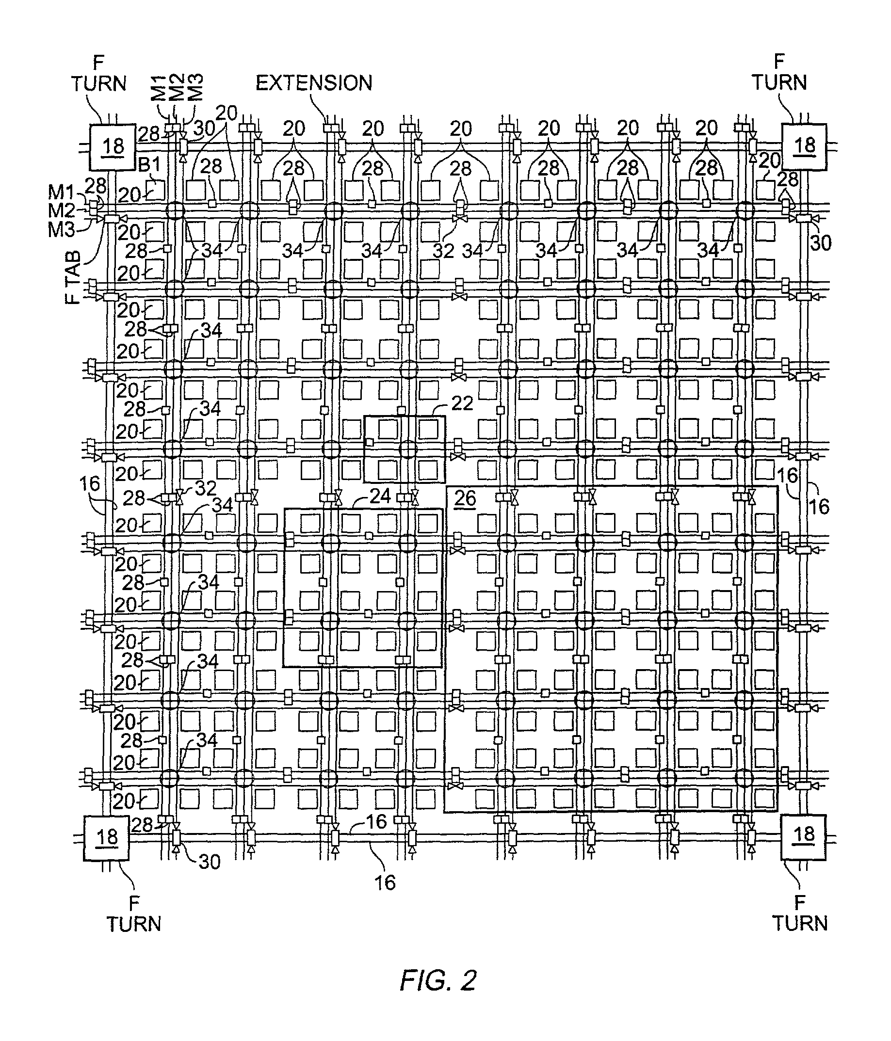
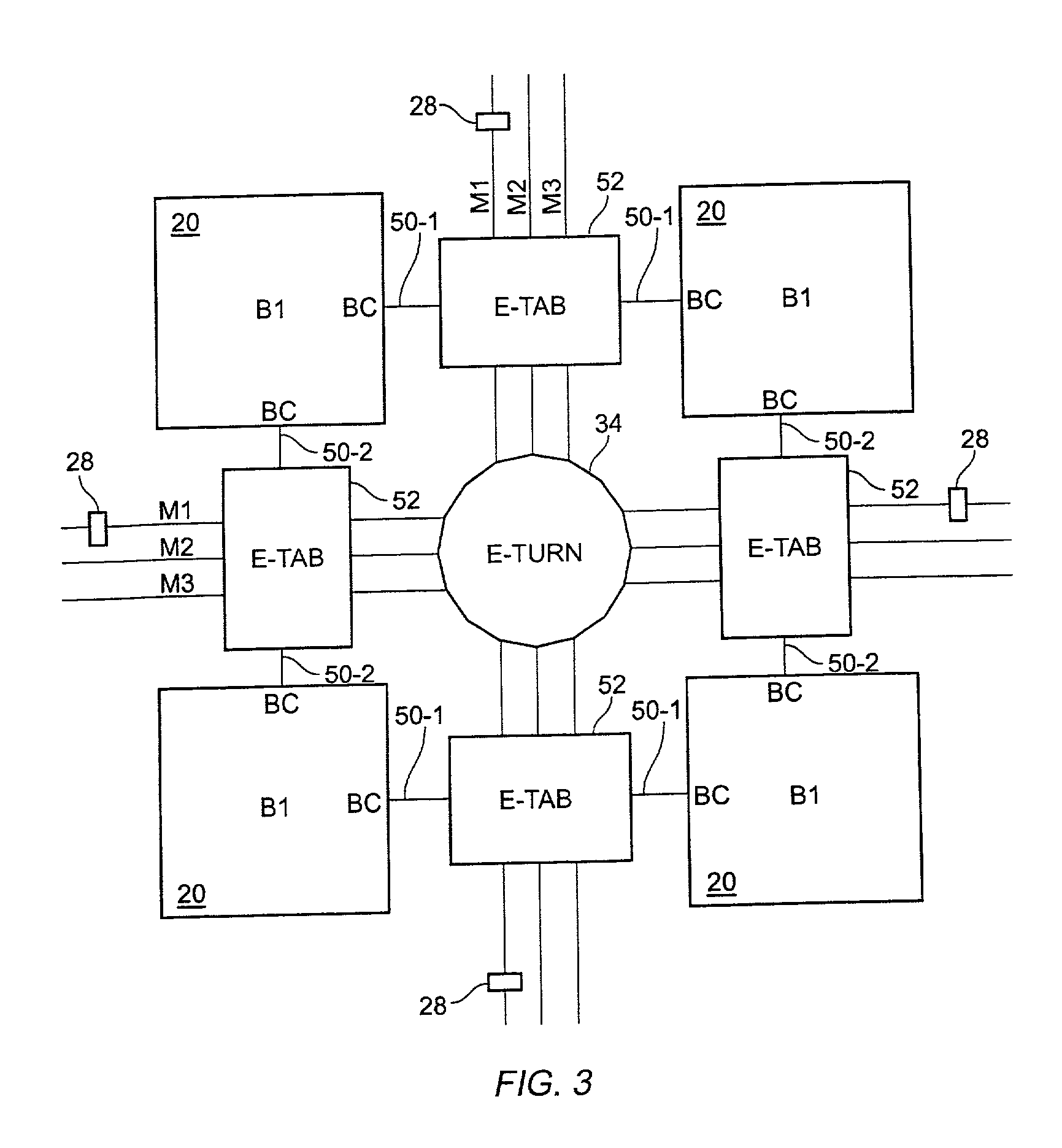
[0021] The present invention is directed to aspects of a semi-hierarchical architecture implemented in an FPGA having top, middle and low levels. In a semi-hierarchical architecture according to the present invention, the three levels of the architecture may be coupled to one another as in a hierarchy or the routing resources in each of the three levels may be extended to similar architectural groups in the same level of the architecture. The semi-hierarchical nature of the FPGA architecture according to the present invention significantly improves the place and route of nets or circuits in the lowest level of the architecture and in the connection of these nets to higher levels in the semi-hierarchical architecture. To better understa...
PUM
 Abstract
Description
Claims
Application Information