Exposure pattern data generation apparatus associated with standard cell library and charged beam exposure

a technology of data generation apparatus and charge beam, which is applied in the direction of photomechanical apparatus, instruments, therapy, etc., can solve the problems of inability to achieve desired throughput disadvantageously, inability to conduct exposure to the other, and inability to obtain desired throughput disadvantageously

Inactive Publication Date: 2001-10-11
KK TOSHIBA
View PDF5 Cites 27 Cited by
  • Summary
  • Abstract
  • Description
  • Claims
  • Application Information

AI Technical Summary

Problems solved by technology

However, since the pattern is divided into many fine rectangular shots and exposure is repeatedly conducted, time required for exposure disadvantageously becomes long and desired throughput cannot be disadvantageously obtained.
Conventionally, therefore, CP exposure is conducted to a pattern such as the pattern of a memory cell which has a large number of times of conducting exposure repeatedly; however, CP exposure cannot be conducted to the other patterns and only VSB exposure, though exposure time is long for VSB exposure, is applicable thereto.
Some logic products cannot obtain the effect of improving throughput even if conducting CP exposure.

Method used


Image

  • Exposure pattern data generation apparatus associated with standard cell library and charged beam exposure
  • Exposure pattern data generation apparatus associated with standard cell library and charged beam exposure
  • Exposure pattern data generation apparatus associated with standard cell library and charged beam exposure

Examples


example 1

of Generating Exposure Pattern Data

[0115] The standard cell libraries 1 and 2 used in this example of generating exposure pattern data include about 400 standard cells. If all of the standard cells can be placed as characters on a CP aperture 44 or an aperture block 3, they can be subjected to CP exposure using the same standard cell libraries 1 and 2 for products designed by automatic P&R.

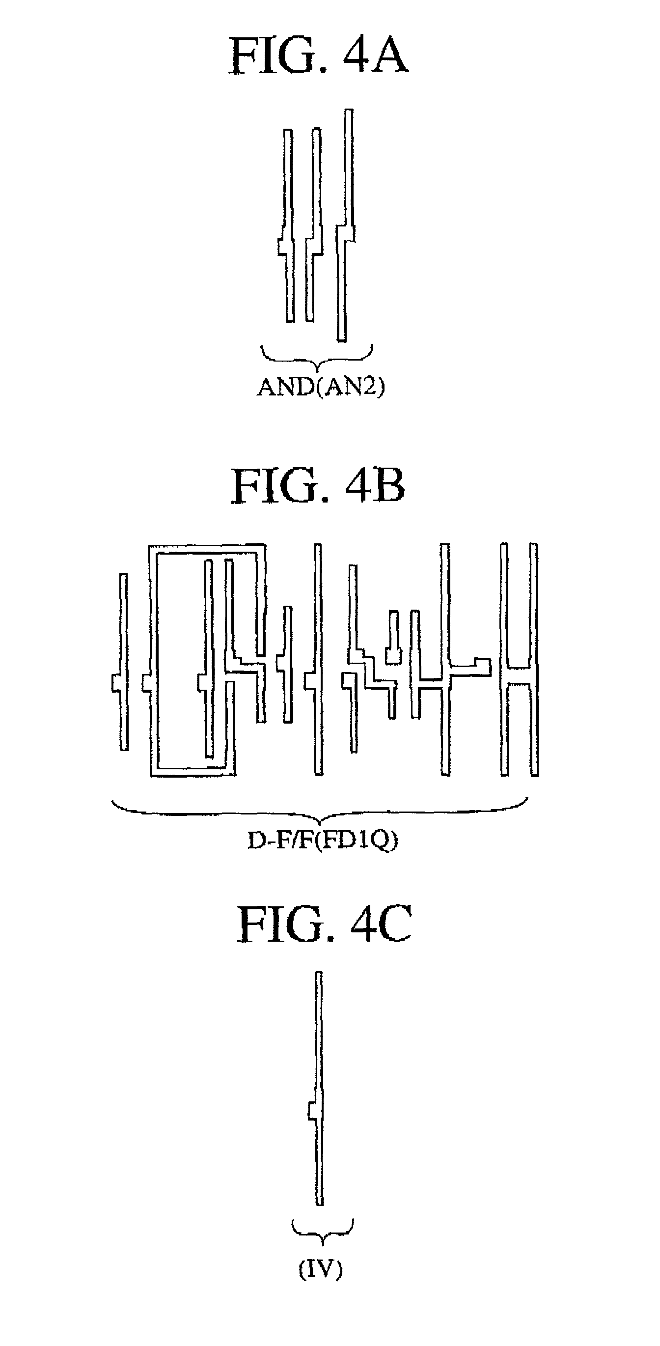
[0116] As for a portion designed by automatic P&R of a certain functional block of a certain logic product among these products, actual design data was examined. The lists of standard cells used in this functional block are shown in FIGS. 15A and 15B. Although 101 types of standard cells of No. 1 to No. 101 are actually included, FIGS. 15A and 15B show 83 types only. Here, the pattern of the gate layer of the cell named FD1Q of No. 1 is the D.F / F circuit shown in FIG. 45. Likewise, AN2 of No. 7 and IV of No. 28 are the AND circuit shown in FIG. 4A and the inverter shown in FIG. 4C, respectively.

[0...

example 2

of Generating Exposure Pattern Data

[0151] Next, a method of generating pattern data 30 suited for CP type electron beam exposure will be described. The generation method is conducted according to a flow chart shown in FIG. 14. By way of example, description will be given to a case of generating pattern data 30 on a certain semiconductor device B while a CP aperture 44 is prepared.

[0152] As shown in FIG. 20, if there exists a CP aperture 44 manufactured for use in a semiconductor device A, pattern data 30 on another semiconductor device B is generated using this CP aperture 44. The allowed exposure throughput of the device B is a minimum of 10 wafers / h. While presuming process and an electron beam exposure to be used, the number of shots of the device A was calculated and converted into throughput of 12 wafers / h.

[0153] First, in the step sit of FIG. 14, logic synthesis is conducted In the form of a logic expression described in the logic design shown in FIG. 9 using the CP aperture w...


PUM

PropertyMeasurementUnit
heightsaaaaaaaaaa
heightaaaaaaaaaa
widthaaaaaaaaaa

Abstract

Logic synthesis is conducted for CP apertures 44 using standard cells corresponding to shaping holes 4 used in logic design of a system and placed at first placement positions on the respective CP apertures 44. A CP aperture 44 used for exposure is selected from among the CP apertures for which logic synthesis has been conducted. Second placement positions of the standard cells on a substrate which standard cells correspond to the shaping holes 4 provided on the selected CP aperture 44 and wiring routes the standard cells are calculated.

Description

[0001] The subject application is related to subject matter disclosed in the Japanese Patent Application 2000-087930 filed in Mar. 28, 2000 in Japan, to which the subject application claims priority under the Paris Convention and which is incorporation by reference herein.[0002] 1. Field of the Invention[0003] The present invention relates to a method of generating the fine pattern of a semiconductor device or a photomask using charged electron beams or charged ion beams and particularly relates to charged beam exposure of a character projection (CP) type.[0004] 2. Description of the Related Art[0005] With an electron beam exposure technique, it is possible to process a fine pattern in sub-micrometers or less which cannot be manufactured by photolithography. The electron beam exposure technique is, therefore, essential to a semiconductor processing technique required to manufacture a more miniaturized, higher integrated, more complicated semiconductor. Invariable shaped beam (VSB) e...

Claims


Application Information

Patent Timeline
Patent Type & Authority Applications(United States)
IPC IPC(8): G03F1/68G03F1/70G03F7/20H01J37/302H01L21/027H01L21/82
CPCB82Y10/00B82Y40/00H01J37/3026H01J37/3174H01J2237/31776
Inventor INANAMI, RYOICHIMAGOSHI, SHUNKO
Owner KK TOSHIBA
Why Eureka
Try Eureka