Liquid treatment equipment, liquid treatment method, semiconductor device manufacturing method, and semiconductor device manufacturing equipment

a technology of semiconductor devices and equipment, applied in the direction of electrolysis components, cleaning using liquids, chemical instruments and processes, etc., can solve the problems of difficult real-time measurement, material repressing plating formation, organic polymer materials, etc., and achieve the effect of reducing the difficulty of bia hole penetration

Inactive Publication Date: 2001-11-08
TOKYO ELECTRON LTD
View PDF16 Cites 6 Cited by
  • Summary
  • Abstract
  • Description
  • Claims
  • Application Information

AI Technical Summary

Problems solved by technology

On the other hand, the material repressing the plating formation, organic polymer material for instance, is relatively large in particle diameter and enters into the trenches or bia holes with difficulty.
Though the concentration of the additive agent in the plating solution is measured by the use of CVS (Cyclic Voltametric Stripper), it is insufficient in view of accuracy and furthermore at present it is difficult to implement a real time measurement.
Furthermore, each time as the plating solution is used in the plating treatment, the additive agent is consumed and lost.
However, due to remaining chemical change matter and decomposition products, each time as the additive agent is added, the plating solution deteriorates in its quality.
(consumption burden of the additive agent and plating solution).
When implementing the plating treatment on the oxidized seed layer, the formed film becomes poor in its plating quality.

Method used


Image

  • Liquid treatment equipment, liquid treatment method, semiconductor device manufacturing method, and semiconductor device manufacturing equipment
  • Liquid treatment equipment, liquid treatment method, semiconductor device manufacturing method, and semiconductor device manufacturing equipment
  • Liquid treatment equipment, liquid treatment method, semiconductor device manufacturing method, and semiconductor device manufacturing equipment

Examples


first embodiment

[0071] In the following, liquid treatment equipment that is a first embodiment of the present invention will be explained. The liquid treatment equipment involving the present embodiment is constituted of a plating unit as part of a systemized plating equipment and a plating solution regeneration unit for readjusting the plating solution that is repeatedly used in the plating treatment unit and deteriorated in the plating capacity.

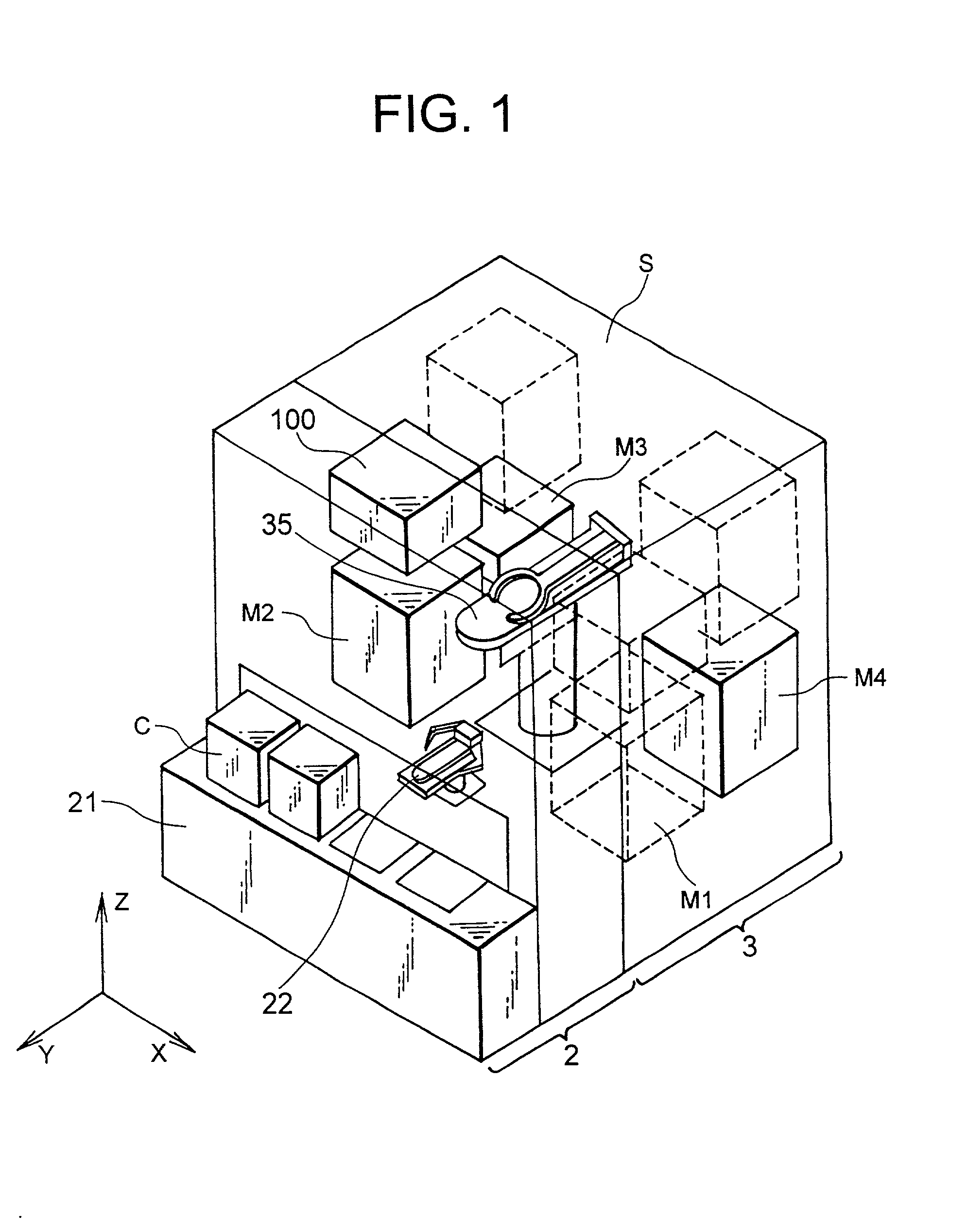
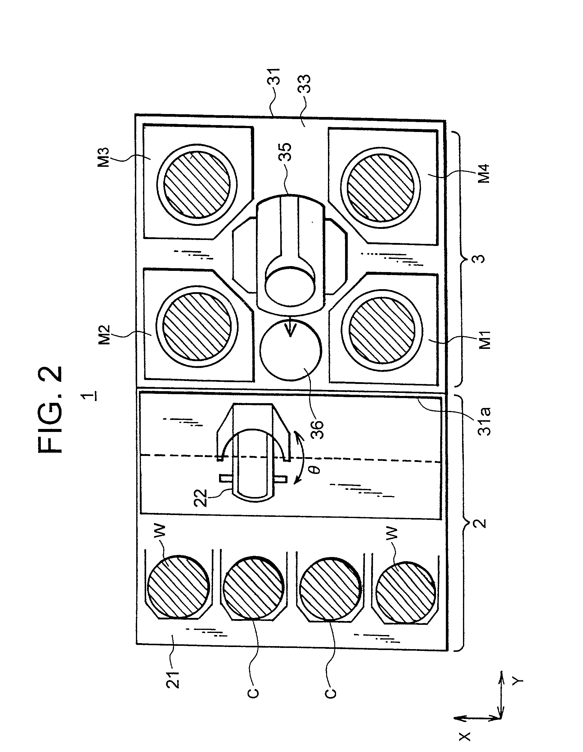
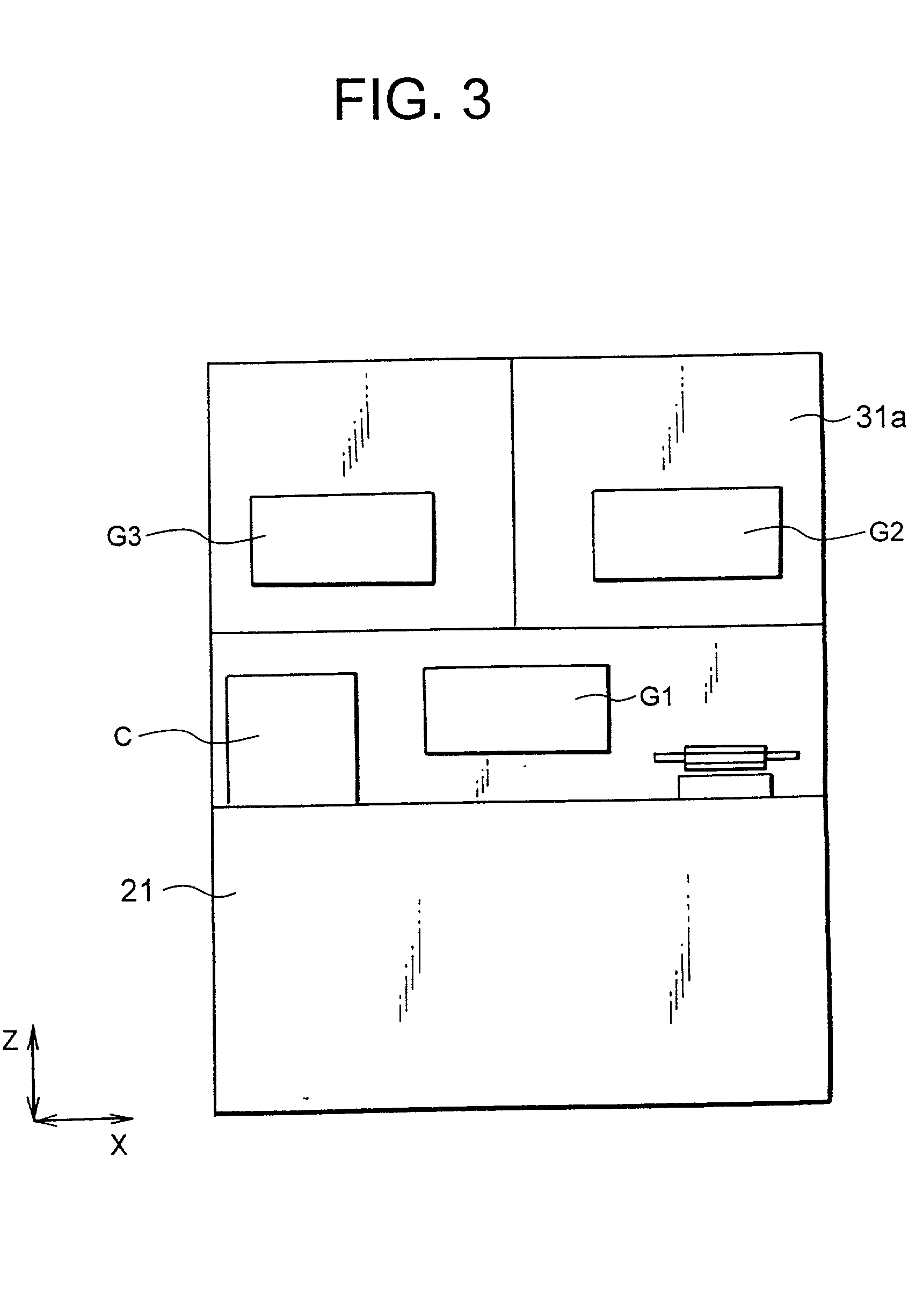
[0072] First, the systemized plating equipment will be explained with reference to FIGS. 1 through 4. FIG. 1 is a perspective view of the systemized plating equipment, FIG. 2 being a plan view of the same plating equipment, FIG. 3 being a front view of the same plating equipment, FIG. 4 being a side view of the same plating equipment.

[0073] As shown in FIGS. 1 through 4, this plating equipment 1 is constituted of a carrier station 2 for carrying in or out or transferring a wafer W and a process station 3 for implementing actual steps of treatment to the wa...

second embodiment

[0161] In the following, a second embodiment of the present invention will be explained with reference to FIG. 11. Of the present embodiment, the content duplicating with the first embodiment is omitted from explanation. FIG. 11 is a schematic vertical section showing a configuration of liquid treatment equipment that is the second embodiment of the present invention. As shown in the same figure, in the present embodiment, below the inner bath 42a the reaction product removal unit is disposed.

[0162] To the inner bath 42a of the plating unit M1, one end of piping 190 is connected. Furthermore, the other end thereof 190 is connected to the circulation piping 46, the plating solution exhausted from the inner bath 42a being again returned to the inner bath 42a.

[0163] In the piping 190, as the reaction product removal unit, a membrane filter 191 for instance is disposed. For the membrane filter 191, a filter of coarseness capable of capturing the impurities such as for instance the decom...

third embodiment

[0168] FIG. 12 is a vertical section schematically showing a configuration of an apparatus for carrying out the step of coating a treatment agent used as a third embodiment of the present invention. The apparatus applies a treatment agent in liquid from above on a surface of a wafer W to treat. A chemical liquid containing the treatment agent is supplied through a chemical liquid supply pipe 217 by means of a chemical liquid supply nozzle 216 on a surface to treat of a wafer W. In the following explanation of the present embodiment, the "treatment agent" is one that has the identical function with the "additive agent" mentioned in the first and second embodiment.

[0169] The wafer W to teat, absorbed and held by a spin chuck 213, is disposed to be freely rotatable due to a level rotation of a spin chuck 214 axis. Due to the rotation of the spin chuck 213, the wafer W to treat is rotated. The chemical liquid supplied by means of the chemical liquid supply nozzle 216 is spread along a r...


PUM

PropertyMeasurementUnit
thicknessaaaaaaaaaa
diameteraaaaaaaaaa
diameteraaaaaaaaaa

Abstract

Providing liquid treatment equipment capable of largely reducing a frequency of discarding a treatment solution as a whole and capable of implementing smooth and high quality liquid treatment with less manufacturing burden. Equipment comprises a treatment solution bath capable of accommodating a treatment solution for implementing liquid treatment to a substrate to treat, a treatment solution circulating system circulating the accommodated treatment solution between the outside of the treatment solution bath, and a product removal unit removing a reaction product due to the liquid treatment contained in the circulated treatment solution. By circulating the accommodated treatment solution between the outside of the treatment solution bath, reaction products contained in the circulated treatment solution are removed by means of the product removal unit. Thereby, a chemical change substance and a decomposition product remaining in a treatment solution can be removed, resulting in preventing a treatment solution from deteriorating.

Description

[0001] 1. Field of the Invention[0002] The present invention relates to liquid treatment equipment for implementing treatment in liquid on a surface of a substrate to treat and a liquid treatment method therefor, and a semiconductor device manufacturing method useful for implementing such liquid treatment and semiconductor device manufacturing equipment useful therefor. In particular, the present invention relates to liquid treatment equipment suitable for implementing smooth and high quality liquid treatment with less manufacturing burden and a liquid treatment method suitable therefor, and a semiconductor device manufacturing method useful in implementing such liquid treatment and semiconductor device manufacturing equipment useful therefor.[0003] 2. Description of the Related Art[0004] Recently, a liquid treatment step in a manufacturing process of semiconductor devices or liquid crystal devices, with an increase of demands for finer processing in the manufacture of semiconductor...

Claims


Application Information

Patent Timeline
Patent Type & Authority Applications(United States)
IPC IPC(8): C25D21/18H01L21/00H01L21/288
CPCC25D21/18H01L21/2885H01L21/67051H01L21/6715H01L21/67167H01L21/67178H01L21/6723Y10S134/902H01L21/00
Inventor MARUMO, YOSHINORIKATO, YOSHINORISATO, HIROSHIPARK, KYUNGHO
Owner TOKYO ELECTRON LTD
Why Eureka
Try Eureka